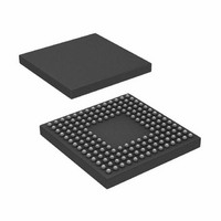
ADSP-BF531SBBC400 Analog Devices Inc, ADSP-BF531SBBC400 Datasheet - Page 8

ADSP-BF531SBBC400
Manufacturer Part Number
ADSP-BF531SBBC400
Description
IC,MICROPROCESSOR,32-BIT,CMOS,BGA,160PIN,PLASTIC
Manufacturer
Analog Devices Inc
Series
Blackfin®r
Type
Fixed Pointr
Datasheet
1.ADSP-BF531SBSTZ400.pdf
(12 pages)
Specifications of ADSP-BF531SBBC400
Rohs Status
RoHS non-compliant
Interface
SPI, SSP, UART
Clock Rate
400MHz
Non-volatile Memory
ROM (1 kB)
On-chip Ram
52kB
Voltage - I/o
1.8V, 2.5V, 3.3V
Voltage - Core
1.20V
Operating Temperature
-40°C ~ 85°C
Mounting Type
Surface Mount
Package / Case
160-CSPBGA
Device Core Size
16b
Architecture
Modified Harvard
Format
Fixed Point
Clock Freq (max)
400MHz
Mips
400
Device Input Clock Speed
400MHz
Operating Supply Voltage (typ)
1.2/1.8/2.5/3.3V
Operating Supply Voltage (min)
0.8/1.75V
Operating Supply Voltage (max)
1.32/3.6V
Operating Temp Range
-40C to 85C
Operating Temperature Classification
Industrial
Mounting
Surface Mount
Pin Count
160
Package Type
CSPBGA
Package
160CSP-BGA
Numeric And Arithmetic Format
Fixed-Point
Maximum Speed
400 MHz
Device Million Instructions Per Second
400 MIPS
For Use With
ADZS-BF533-EZLITE - KIT W/BOARD EVAL FOR ADSP-BF533
Lead Free Status / Rohs Status
Not Compliant
Available stocks
Company
Part Number
Manufacturer
Quantity
Price
Company:
Part Number:
ADSP-BF531SBBC400
Manufacturer:
ADI
Quantity:
329
Company:
Part Number:
ADSP-BF531SBBC400
Manufacturer:
Analog Devices Inc
Quantity:
10 000
Part Number:
ADSP-BF531SBBC400
Manufacturer:
ADI/亚德诺
Quantity:
20 000
ADSP-BF531/BF532/BF533
7.
8.
9.
10.
05000166 - PPI Data Lengths between 8 and 16 Do Not Zero Out Upper Bits:
05000167 - Turning SPORTs on while External Frame Sync Is Active May Corrupt Data:
05000179 - PPI_COUNT Cannot Be Programmed to 0 in General Purpose TX or RX Modes:
DESCRIPTION:
For PPI data lengths greater than 8 and less than 16, the upper bits received into memory that are not part of the PPI data should be zero.
For example, if the user is using 10-bit PPI data length, the upper 6 bits in memory should be zero. Instead, the PPI captures whatever
data is on the upper 6 PPI data pins (muxed as PFx pins).
WORKAROUND:
The software workaround is to mask out the upper 6 bits when processing received data.
APPLIES TO REVISION(S):
0.3, 0.4, 0.5, 0.6
DESCRIPTION:
The SPORTs are level sensitive to External Frame Syncs. If a SPORT is configured for External Frame Syncs and the frame sync is active
when the SPORT is first enabled, the SPORT will start receiving data immediately when enabled. This may occur in the middle of a frame,
causing incorrect data to be received.
This anomaly also applies to Stereo Serial Modes (I2S and variants), except in the case where either the LRFS or the RRFST bit is set (not
both).
WORKAROUND:
Hold off external Frame syncs until the SPORT is fully enabled. If you use a serial device with external frame syncs that can't be held off
until the SPORT is enabled, a programmable flag pin can be connected to the Frame Sync. The PFx pin can be programmed to continually
sample the SPORT Frame Sync and then enable the SPORT when the RFS / TFS signals are in the inactive state.
For Stereo Serial Modes, either set the LRFS or the RRFST bit (not both), if possible.
APPLIES TO REVISION(S):
0.3, 0.4, 0.5, 0.6
DESCRIPTION:
In General Purpose modes, the PPI must receive or transmit blocks of at least 2 words. Single word transfers (PPI_COUNT value of 0) are
not functional.
WORKAROUND:
None
APPLIES TO REVISION(S):
0.3, 0.4
DESCRIPTION:
In self-triggered, continuous sampling operation of the PPI, the delay count specified in the PPI_DELAY register is ignored. As soon as this
mode is enabled, data is transferred.
WORKAROUND:
If a delay is needed, either ignore received data in software or use a mode with at least one frame sync.
APPLIES TO REVISION(S):
0.3, 0.4, 0.5, 0.6
05000180 - PPI_DELAY Not Functional in PPI Modes with 0 Frame Syncs:
NR003532D | Page 8 of 45 | July 2008
Silicon Anomaly List


