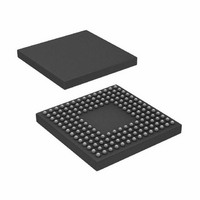
ADSP-BF531SBBC400 Analog Devices Inc, ADSP-BF531SBBC400 Datasheet - Page 41

ADSP-BF531SBBC400
Manufacturer Part Number
ADSP-BF531SBBC400
Description
IC,MICROPROCESSOR,32-BIT,CMOS,BGA,160PIN,PLASTIC
Manufacturer
Analog Devices Inc
Series
Blackfin®r
Type
Fixed Pointr
Datasheet
1.ADSP-BF531SBSTZ400.pdf
(12 pages)
Specifications of ADSP-BF531SBBC400
Rohs Status
RoHS non-compliant
Interface
SPI, SSP, UART
Clock Rate
400MHz
Non-volatile Memory
ROM (1 kB)
On-chip Ram
52kB
Voltage - I/o
1.8V, 2.5V, 3.3V
Voltage - Core
1.20V
Operating Temperature
-40°C ~ 85°C
Mounting Type
Surface Mount
Package / Case
160-CSPBGA
Device Core Size
16b
Architecture
Modified Harvard
Format
Fixed Point
Clock Freq (max)
400MHz
Mips
400
Device Input Clock Speed
400MHz
Operating Supply Voltage (typ)
1.2/1.8/2.5/3.3V
Operating Supply Voltage (min)
0.8/1.75V
Operating Supply Voltage (max)
1.32/3.6V
Operating Temp Range
-40C to 85C
Operating Temperature Classification
Industrial
Mounting
Surface Mount
Pin Count
160
Package Type
CSPBGA
Package
160CSP-BGA
Numeric And Arithmetic Format
Fixed-Point
Maximum Speed
400 MHz
Device Million Instructions Per Second
400 MIPS
For Use With
ADZS-BF533-EZLITE - KIT W/BOARD EVAL FOR ADSP-BF533
Lead Free Status / Rohs Status
Not Compliant
Available stocks
Company
Part Number
Manufacturer
Quantity
Price
Company:
Part Number:
ADSP-BF531SBBC400
Manufacturer:
ADI
Quantity:
329
Company:
Part Number:
ADSP-BF531SBBC400
Manufacturer:
Analog Devices Inc
Quantity:
10 000
Part Number:
ADSP-BF531SBBC400
Manufacturer:
ADI/亚德诺
Quantity:
20 000
Silicon Anomaly List
71.
72.
DESCRIPTION:
When the VR_CTL register is programmed to contain VLEV values of 0xA, 0xB, or 0xC (1.05V, 1.10V, and 1.15V, respectively), the actual
Vddint applied to the core through the regulator may drop below the specified tolerance of -5%.
This issue only occurs on parts in LQFP packages.
WORKAROUND:
Either avoid programming these values or program the regulator to the next highest setting to ensure that the Vddint remains above the
minimum threshold for the core clock that the application is running.
APPLIES TO REVISION(S):
0.3, 0.4, 0.5
DESCRIPTION:
When configured in multi-channel mode with channel 0 disabled, DMA transmit data will be sent to the wrong SPORT channel if all of the
following criteria are met:
1) External Receive Frame Sync (IRFS = 0 in SPORTx_RCR1)
2) Window Offset = 0 (WOFF = 0 in SPORTx_MCMC1)
3) Multichannel Frame Delay = 0 (MFD = 0 in SPORTx_MCMC2)
4) DMA Transmit Packing Disabled (MCDTXPE = 0 in SPORTx_MCMC2)
When this specific configuration is used, the multi-channel transmit data gets corrupted because whatever is in the channel 0 placeholder
in non-packed mode gets sent first, even though channel 0 is disabled. The result is a one-word data shift in the output window, which
repeats for each subsequent window in the serial stream. For example, if the non-packed transmit buffer is {0, 1, 2, 3, 4, 5, 6, 7}, and the
window size is 8 channels with channel 0 disabled and channels 1-7 enabled to transmit, the expected data sequence in a series of output
windows is:
1234567--1234567--1234567--1234567
With this anomaly, the output looks like this instead:
0123456--7012345--6701234--5670123
WORKAROUND:
There are several possible workarounds to this:
1) Disable Multichannel Mode
2) Use Internal Receive Frame Syncs
3) Use a Multichannel Frame Delay > 0
4) Use a Window Offset > 0
5) Enable DMA Transmit Packing
6) Do not disable Channel 0
APPLIES TO REVISION(S):
0.3, 0.4, 0.5
05000319 - Internal Voltage Regulator Values of 1.05V, 1.10V and 1.15V Not Allowed for LQFP Packages:
05000357 - Serial Port (SPORT) Multichannel Transmit Failure when Channel 0 Is Disabled:
NR003532D | Page 41 of 45 | July 2008
ADSP-BF531/BF532/BF533


