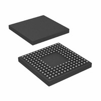
ADSP-BF531SBBC400 Analog Devices Inc, ADSP-BF531SBBC400 Datasheet - Page 32

ADSP-BF531SBBC400
Manufacturer Part Number
ADSP-BF531SBBC400
Description
IC,MICROPROCESSOR,32-BIT,CMOS,BGA,160PIN,PLASTIC
Manufacturer
Analog Devices Inc
Series
Blackfin®r
Type
Fixed Pointr
Datasheet
1.ADSP-BF531SBSTZ400.pdf
(12 pages)
Specifications of ADSP-BF531SBBC400
Rohs Status
RoHS non-compliant
Interface
SPI, SSP, UART
Clock Rate
400MHz
Non-volatile Memory
ROM (1 kB)
On-chip Ram
52kB
Voltage - I/o
1.8V, 2.5V, 3.3V
Voltage - Core
1.20V
Operating Temperature
-40°C ~ 85°C
Mounting Type
Surface Mount
Package / Case
160-CSPBGA
Device Core Size
16b
Architecture
Modified Harvard
Format
Fixed Point
Clock Freq (max)
400MHz
Mips
400
Device Input Clock Speed
400MHz
Operating Supply Voltage (typ)
1.2/1.8/2.5/3.3V
Operating Supply Voltage (min)
0.8/1.75V
Operating Supply Voltage (max)
1.32/3.6V
Operating Temp Range
-40C to 85C
Operating Temperature Classification
Industrial
Mounting
Surface Mount
Pin Count
160
Package Type
CSPBGA
Package
160CSP-BGA
Numeric And Arithmetic Format
Fixed-Point
Maximum Speed
400 MHz
Device Million Instructions Per Second
400 MIPS
For Use With
ADZS-BF533-EZLITE - KIT W/BOARD EVAL FOR ADSP-BF533
Lead Free Status / Rohs Status
Not Compliant
Available stocks
Company
Part Number
Manufacturer
Quantity
Price
Company:
Part Number:
ADSP-BF531SBBC400
Manufacturer:
ADI
Quantity:
329
Company:
Part Number:
ADSP-BF531SBBC400
Manufacturer:
Analog Devices Inc
Quantity:
10 000
Part Number:
ADSP-BF531SBBC400
Manufacturer:
ADI/亚德诺
Quantity:
20 000
ADSP-BF531/BF532/BF533
56.
57.
DESCRIPTION:
If a write to any I/O data register (data, clear, set and toggle registers) occurs one system clock cycle after an edge is detected on an edge-
triggered interrupt, then the bit may be cleared one system clock cycle after it has been set.
If the bit has been programmed to generate an interrupt, then the interrupt will occur, but there will be no indication of which bit
signalled the interrupt. The interrupt will be lost if the core clock is not running or if the SIC_IMASK bit is not set to enable the interrupt.
WORKAROUND:
If only one edge-sensitive source is assigned to one interrupt, it can be assumed to be the source of the interrupt and a read instruction of
SIC_ISR and the I/O registers is not required. Note that all interrupts are properly executed, when enabled.
Use level-sensitive interrupts instead of edge-sensitive interrupts. Toggle the polarity between received edges to prevent re-entry of the
interrupt service routine and to sensitize for the next edge. This is applicable when the latency between two edges is sufficient to serve
the interrupt service routine or can be used for request lines. Toggling polarity can be used when looking for both edges. For only one
edge, however, the other interrupt must be ignored.
APPLIES TO REVISION(S):
0.3, 0.4, 0.5
DESCRIPTION:
If a peripheral (PPI, SPORT, SPI, etc.) is disabled while DMA is running and before the associated DMA channel is disabled, the DMA system
may be corrupted. In applications with multiple DMA channels running concurrently, this anomaly manifests itself with missing data or
shuffled data being transferred. Although the anomaly also affects applications with a single DMA channel, its effects may not be visible if
the peripheral is being shut down by the user code.
WORKAROUND:
If the DMA channel is running, disable the peripheral's associated DMA channel before disabling the peripheral itself.
If the DMA channel is stopped, the peripheral must be disabled before the associated DMA channel is disabled. When a channel is
disabled, the DMA unit ignores the peripheral interrupt and passes it directly to the interrupt controller, thus generating spurios
interrupts.
APPLIES TO REVISION(S):
0.3, 0.4, 0.5
05000277 - Writes to an I/O Data Register One SCLK Cycle after an Edge Is Detected May Clear Interrupt:
05000278 - Disabling Peripherals with DMA Running May Cause DMA System Instability:
NR003532D | Page 32 of 45 | July 2008
Silicon Anomaly List


