ADUC7122BBCZ-RL Analog Devices Inc, ADUC7122BBCZ-RL Datasheet - Page 18
ADUC7122BBCZ-RL
Manufacturer Part Number
ADUC7122BBCZ-RL
Description
PRECISION ANALOG MCU I.C
Manufacturer
Analog Devices Inc
Series
MicroConverter® ADuC7xxxr
Datasheet
1.ADUC7122BBCZ.pdf
(96 pages)
Specifications of ADUC7122BBCZ-RL
Core Processor
ARM7
Core Size
16/32-Bit
Speed
41.78MHz
Connectivity
I²C, SPI, UART/USART
Peripherals
POR, PWM, WDT
Number Of I /o
32
Program Memory Size
126KB (63K x 16)
Program Memory Type
FLASH
Ram Size
8K x 8
Voltage - Supply (vcc/vdd)
3 V ~ 3.6 V
Data Converters
A/D 13x12b, D/A 12x12b
Oscillator Type
Internal
Operating Temperature
-10°C ~ 95°C
Package / Case
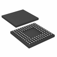
108-LFBGA, CSPBGA
Lead Free Status / RoHS Status
Lead free / RoHS Compliant
Eeprom Size
-
Lead Free Status / RoHS Status
Lead free / RoHS Compliant
Other names
ADUC7122BBCZ-RL
ADUC7122BBCZ-RLTR
ADUC7122BBCZ-RLTR
Available stocks
Company
Part Number
Manufacturer
Quantity
Price
Company:

Part Number:
ADUC7122BBCZ-RL
Manufacturer:
Analog Devices Inc
Quantity:
10 000


ADuC7122
Pin No.
A9
A11
A10
B12
B11
B10
B9
M1
M6
L1
M7
M12
B6
L12
C7
B7
G1
G12
F1
F12
H1
J1
H12
J12
G2
H2
D10
C10
F10
E10
1
I = input, I/O = input/output, AI/O = analog input/output, NC = no connect, AO = analog output, AI = analog input, DI = digital input, DO = digital output, S = supply.
Mnemonic
NC
NC
NC
NC
NC
AGND
AGND
AGND
AGND
AVDD
AVDD
AGND
AGND
AVDD
NC
REG_PWR
LVDD
LVDD
DGND
DGND
IOVDD
IOGND
IOVDD
IOGND
XTALO
XTALI
TDO/P1.3/PLAO[14]
TDI/P1.2/PLAO[15]
TCK
TMS
S
S
Type
NC
NC
NC
NC
NC
S
S
S
S
S
S
S
S
S
NC
S
S
S
S
S
S
S
DO
DI
DO
DI
DI
DI
1
Description
No Connect.
No Connect.
No Connect.
No Connect.
No Connect.
Analog Ground.
Analog Ground.
Analog Ground.
Analog Ground.
Analog Supply (3.3 V).
Analog Supply (3.3 V).
Analog Ground.
Analog Ground.
Analog Supply (3.3 V).
No Connect.
Output of 2.5 V On-Chip Regulator. A 470 nF capacitor to DGND must be connected to
this pin.
Output of 2.6 V On-Chip LDO Regulator. A 470 nF capacitor to DGND must be
connected to this pin.
Output of 2.6 V On-Chip LDO Regulator. A 470 nF capacitor to DGND must be
connected to this pin.
Digital ground.
Digital ground.
3.3 V GPIO Supply.
3.3 V GPIO Ground.
3.3 V GPIO Supply.
3.3 V GPIO Ground.
Output from the Crystal Oscillator Inverter. If an external crystal is not being used, this
pin can be left unconnected.
Input to the Crystal Oscillator Inverter and Input to the Internal Clock Generator
Circuits. If an external crystal is not being used, this pin should be connected to the
DGND system ground.
JTAG Test Port Output, Test Data Out (TDO). Debug and download access.
General-Purpose Input and Output Port 1.3 (P1.3).
Output of PLA Element 14 (PLAO[14]). This pin should not be used as a GPIO when
debugging via the JTAG interface.
JTAG Test Port Input, Test Data In (TDI). Debug and download access.
General-Purpose Input and Output Port 1.2 (P1.2).
Output of PLA Element 15 (PLAO[15]). This pin should not be used as a GPIO when
debugging via the JTAG interface.
JTAG Test Port Input, Test Clock. Debug and download access.
JTAG Test Port Input, Test Mode Select. Debug and download access.
Rev. 0 | Page 18 of 96
Related parts for ADUC7122BBCZ-RL
Image
Part Number
Description
Manufacturer
Datasheet
Request
R

Part Number:
Description:
±1.7g Dual-Axis IMEMS Accelerometer Evaluation Board
Manufacturer:
Analog Devices Inc
Datasheet:

Part Number:
Description:
Inertial Sensor Evaluation System
Manufacturer:
Analog Devices Inc
Datasheet:
Part Number:
Description:
Manufacturer:
Analog Devices Inc
Datasheet:
Part Number:
Description:
Manufacturer:
Analog Devices Inc
Datasheet:
Part Number:
Description:
Manufacturer:
Analog Devices Inc
Datasheet:
Part Number:
Description:
Manufacturer:
Analog Devices Inc
Datasheet:
Part Number:
Description:
Manufacturer:
Analog Devices Inc
Datasheet:
Part Number:
Description:
Manufacturer:
Analog Devices Inc
Datasheet:
Part Number:
Description:
Manufacturer:
Analog Devices Inc
Datasheet:
Part Number:
Description:
Manufacturer:
Analog Devices Inc
Datasheet:
Part Number:
Description:
Manufacturer:
Analog Devices Inc
Datasheet:
Part Number:
Description:
Manufacturer:
Analog Devices Inc
Datasheet:
Part Number:
Description:
Manufacturer:
Analog Devices Inc
Datasheet: