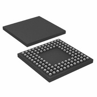
ADUC7122BBCZ-RL Analog Devices Inc, ADUC7122BBCZ-RL Datasheet - Page 76

ADUC7122BBCZ-RL
Manufacturer Part Number
ADUC7122BBCZ-RL
Description
PRECISION ANALOG MCU I.C
Manufacturer
Analog Devices Inc
Series
MicroConverter® ADuC7xxxr
Datasheet
1.ADUC7122BBCZ.pdf
(96 pages)
Specifications of ADUC7122BBCZ-RL
Core Processor
ARM7
Core Size
16/32-Bit
Speed
41.78MHz
Connectivity
I²C, SPI, UART/USART
Peripherals
POR, PWM, WDT
Number Of I /o
32
Program Memory Size
126KB (63K x 16)
Program Memory Type
FLASH
Ram Size
8K x 8
Voltage - Supply (vcc/vdd)
3 V ~ 3.6 V
Data Converters
A/D 13x12b, D/A 12x12b
Oscillator Type
Internal
Operating Temperature
-10°C ~ 95°C
Package / Case
108-LFBGA, CSPBGA
Lead Free Status / RoHS Status
Lead free / RoHS Compliant
Eeprom Size
-
Lead Free Status / RoHS Status
Lead free / RoHS Compliant
Other names
ADUC7122BBCZ-RL
ADUC7122BBCZ-RLTR
ADUC7122BBCZ-RLTR
Available stocks
Company
Part Number
Manufacturer
Quantity
Price
Company:
Part Number:
ADUC7122BBCZ-RL
Manufacturer:
Analog Devices Inc
Quantity:
10 000
ADuC7122
INTERRUPT SYSTEM
There are 27 interrupt sources on the ADuC7122 that are con-
trolled by the interrupt controller. All interrupts are generated
from the on-chip peripherals, except for the software interrupt
(SWI), which is programmable by the user. The ARM7TDMI
CPU core only recognizes interrupts as one of two types: a
normal interrupt request (IRQ) and a fast interrupt request
(FIQ). All the interrupts can be masked separately.
The control and configuration of the interrupt system is
managed through a number of interrupt-related registers. The
bits in each IRQ and FIQ register represent the same interrupt
source, as described in Table 128.
Table 128. IRQ/FIQ
Bit
0
1
2
3
4
5
6
7
8
9
10
11
12
13
14
15
16
17
18
19
20
21
22
23
24
25
26
27
1
Applies to IRQEN, FIQEN, IRQCLR, FIQCLR, IRQSTA, and FIQSTA registers.
Description
All interrupts OR’ed (FIQ only)
Software interrupt
Timer0
Timer1
Timer2 or wake-up timer
Timer3 or watchdog timer
Timer4
Reserved
PSM
Undefined
Flash Control 0
Flash Control 1
ADC
UART
SPI
I2C0 master IRQ
I2C0 slave IRQ
I2C1 master IRQ
I2C1 slave IRQ
XIRQ0 (GPIO IRQ0 )
XIRQ1 (GPIO IRQ1)
XIRQ2 (GPIO IRQ2 )
XIRQ3 (GPIO IRQ3)
PWM
XIRQ4 (GPIO IRQ4 )
XIRQ5 (GPIO IRQ5)
PLA IRQ0
PLA IRQ1
1
MMRs Bit Designations
Rev. 0 | Page 76 of 96
Comments
This bit is set if any FIQ is active
User programmable interrupt source
General-Purpose Timer0
General-Purpose Timer1
General-Purpose Timer2 or wake-up timer
General-Purpose Timer3 or watchdog timer
General-Purpose Timer4
Reserved
Power supply monitor
This bit is not used
Flash controller for Block 0 interrupt
Flash controller for Block 1 interrupt
ADC interrupt source bit
UART interrupt source bit
SPI interrupt source bit
I
I
I
I
External Interrupt 0
External Interrupt 1
External Interrupt 2
External Interrupt 3
PWM trip interrupt source bit
External Interrupt 4
External Interrupt 5
PLA Block 0 IRQ bit
PLA Block 1 IRQ bit
2
2
2
2
C master interrupt source bit
C slave interrupt source bit
C master interrupt source bit
C slave interrupt source bit
The ADuC7122 contains a vectored interrupt controller (VIC)
that supports nested interrupts up to eight levels. The VIC also
allows the programmer to assign priority levels to all interrupt
sources. Interrupt nesting needs to be enabled by setting the
ENIRQN bit in the IRQCONN register. A number of extra
MMRs are used when the full vectored interrupt controller is
enabled.
IRQSTA/FIQSTA should be saved immediately upon entering
the interrupt service routine (ISR) to ensure that all valid
interrupt sources are serviced.


