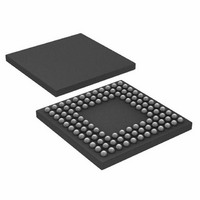
ADUC7122BBCZ-RL Analog Devices Inc, ADUC7122BBCZ-RL Datasheet - Page 31

ADUC7122BBCZ-RL
Manufacturer Part Number
ADUC7122BBCZ-RL
Description
PRECISION ANALOG MCU I.C
Manufacturer
Analog Devices Inc
Series
MicroConverter® ADuC7xxxr
Datasheet
1.ADUC7122BBCZ.pdf
(96 pages)
Specifications of ADUC7122BBCZ-RL
Core Processor
ARM7
Core Size
16/32-Bit
Speed
41.78MHz
Connectivity
I²C, SPI, UART/USART
Peripherals
POR, PWM, WDT
Number Of I /o
32
Program Memory Size
126KB (63K x 16)
Program Memory Type
FLASH
Ram Size
8K x 8
Voltage - Supply (vcc/vdd)
3 V ~ 3.6 V
Data Converters
A/D 13x12b, D/A 12x12b
Oscillator Type
Internal
Operating Temperature
-10°C ~ 95°C
Package / Case
108-LFBGA, CSPBGA
Lead Free Status / RoHS Status
Lead free / RoHS Compliant
Eeprom Size
-
Lead Free Status / RoHS Status
Lead free / RoHS Compliant
Other names
ADUC7122BBCZ-RL
ADUC7122BBCZ-RLTR
ADUC7122BBCZ-RLTR
Available stocks
Company
Part Number
Manufacturer
Quantity
Price
Company:
Part Number:
ADUC7122BBCZ-RL
Manufacturer:
Analog Devices Inc
Quantity:
10 000
Table 28. ADCCON MMR Bit Designations (Address = 0xFFFF0500, Default Value = 0x00000A00)
Bit
31:16
15
14
13:11
10:8
7
6
5
4:3
2:0
Value
0
1
0
1
000
001
010
011
100
101
000
001
010
011
100
101
1
0
1
0
00
01
10
11
000
001
010
011
100
101
110
Other
Description
These bits are reserved.
Positive ADC buffer bypass.
Set to 0 by the user to enable the positive ADC buffer.
Set to 1 by the user to bypass the positive ADC buffer.
Negative ADC buffer bypass.
Set to 0 by the user to enable the negative ADC buffer.
Set to 1 by the user to bypass the negative ADC buffer.
ADC clock speed (f
f
f
f
f
f
f
ADC acquisition time (number of ADC clocks).
2 clocks.
4 clocks.
8 clocks (default value).
16 clocks.
32 clocks.
64 clocks.
Enable conversion.
Set by user to 1 to enable conversion mode.
Cleared by user to 0 to disable conversion mode.
Reserved. This bit should be set to 0 by the user.
ADC power control.
Set by user to 1 to place the ADC in normal mode. The ADC must be powered up for at least 5 μs before it converts correctly.
Cleared by user to 0 to place the ADC in power-down mode.
Conversion mode.
Single-ended mode.
Differential mode.
Pseudo differential mode.
Reserved.
Conversion type.
Enable CONVST pin as a conversion input.
Enable Timer1 as a conversion input.
Enable Timer0 as a conversion input.
Single software conversion. Automatically set to 000 after conversion.
Continuous software conversion.
PLA conversion.
Reserved
Reserved.
ADC
ADC
ADC
ADC
ADC
ADC
/1. This divider is provided to obtain 1 MSPS ADC with an external clock <41.78 MHz.
/2 (default value).
/4.
/8.
/16.
/32.
ADC
= f
CORE
, conversion = 19 ADC clocks + acquisition time).
Rev. 0 | Page 31 of 96
ADuC7122


