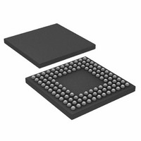
ADUC7122BBCZ-RL Analog Devices Inc, ADUC7122BBCZ-RL Datasheet - Page 30

ADUC7122BBCZ-RL
Manufacturer Part Number
ADUC7122BBCZ-RL
Description
PRECISION ANALOG MCU I.C
Manufacturer
Analog Devices Inc
Series
MicroConverter® ADuC7xxxr
Datasheet
1.ADUC7122BBCZ.pdf
(96 pages)
Specifications of ADUC7122BBCZ-RL
Core Processor
ARM7
Core Size
16/32-Bit
Speed
41.78MHz
Connectivity
I²C, SPI, UART/USART
Peripherals
POR, PWM, WDT
Number Of I /o
32
Program Memory Size
126KB (63K x 16)
Program Memory Type
FLASH
Ram Size
8K x 8
Voltage - Supply (vcc/vdd)
3 V ~ 3.6 V
Data Converters
A/D 13x12b, D/A 12x12b
Oscillator Type
Internal
Operating Temperature
-10°C ~ 95°C
Package / Case
108-LFBGA, CSPBGA
Lead Free Status / RoHS Status
Lead free / RoHS Compliant
Eeprom Size
-
Lead Free Status / RoHS Status
Lead free / RoHS Compliant
Other names
ADUC7122BBCZ-RL
ADUC7122BBCZ-RLTR
ADUC7122BBCZ-RLTR
Available stocks
Company
Part Number
Manufacturer
Quantity
Price
Company:
Part Number:
ADUC7122BBCZ-RL
Manufacturer:
Analog Devices Inc
Quantity:
10 000
ADuC7122
TEMPERATURE SENSOR
The ADuC7122 provides a voltage output from an on-chip
band gap reference proportional to absolute temperature.
This voltage output can also be routed through the front-end
ADC multiplexer (effectively, an additional ADC channel input),
facilitating an internal temperature sensor channel that measures
die temperature.
The internal temperature sensor is not designed for use as
an absolute ambient temperature calculator. It is intended for
use as an approximate indicator of the temperature of the
ADuC7122 die.
The typical temperature coefficient is −1.25 mV/°C.
Table 27. ADC MMRs
Name
ADCCON
ADCCP
ADCCN
ADCSTA
ADCDAT
ADCRST
PGA_GN
Description
ADC control register. Allows the programmer to enable the ADC peripheral to select the mode of operation of the ADC (either
single-ended, pseudo differential, or fully differential mode) and to select the conversion type (see Table 28).
ADC positive channel selection register.
ADC negative channel selection register.
ADC status register. Indicates when an ADC conversion result is ready. The ADCSTA register contains only one bit, ADCREADY
(Bit 0), representing the status of the ADC. This bit is set at the end of an ADC conversion generating an ADC interrupt. It is
cleared automatically by reading the ADCDAT MMR. When the ADC is performing a conversion, the status of the ADC can be
read externally via the ADC
This information is available on P0.2 (see the General-Purpose I/O section) if enabled in the GP0CON register.
ADC data result register. Holds the 12-bit ADC result, as shown Table 32.
ADC reset register. Resets all the ADC registers to their default value.
Gain of PADC0 and PADC1.
Busy
pin. This pin is high during a conversion. When the conversion is finished, ADC
Rev. 0 | Page 30 of 96
ADC MMRs Interface
The ADC is controlled and configured via a number of MMRs
(see Table 27) that are described in detail in Table 28 to Table 34.
1250
1200
1150
1100
1050
1000
–20
Figure 17. ADC Output vs. Temperature
0
20
TEMPERATURE (°C)
40
60
Busy
goes back low.
80
100


