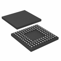
ADUC7122BBCZ-RL Analog Devices Inc, ADUC7122BBCZ-RL Datasheet - Page 52

ADUC7122BBCZ-RL
Manufacturer Part Number
ADUC7122BBCZ-RL
Description
PRECISION ANALOG MCU I.C
Manufacturer
Analog Devices Inc
Series
MicroConverter® ADuC7xxxr
Datasheet
1.ADUC7122BBCZ.pdf
(96 pages)
Specifications of ADUC7122BBCZ-RL
Core Processor
ARM7
Core Size
16/32-Bit
Speed
41.78MHz
Connectivity
I²C, SPI, UART/USART
Peripherals
POR, PWM, WDT
Number Of I /o
32
Program Memory Size
126KB (63K x 16)
Program Memory Type
FLASH
Ram Size
8K x 8
Voltage - Supply (vcc/vdd)
3 V ~ 3.6 V
Data Converters
A/D 13x12b, D/A 12x12b
Oscillator Type
Internal
Operating Temperature
-10°C ~ 95°C
Package / Case
108-LFBGA, CSPBGA
Lead Free Status / RoHS Status
Lead free / RoHS Compliant
Eeprom Size
-
Lead Free Status / RoHS Status
Lead free / RoHS Compliant
Other names
ADUC7122BBCZ-RL
ADUC7122BBCZ-RLTR
ADUC7122BBCZ-RLTR
Available stocks
Company
Part Number
Manufacturer
Quantity
Price
Company:
Part Number:
ADUC7122BBCZ-RL
Manufacturer:
Analog Devices Inc
Quantity:
10 000
ADuC7122
GENERAL-PURPOSE I/O
The ADuC7122 provides 32 general-purpose, bidirectional I/O
(GPIO) pins. All I/O pins are 5 V tolerant, meaning that the
GPIOs support an input voltage of 5 V. In general, many of the
GPIO pins have multiple functions (see Table 84). By default, the
GPIO pins are configured in GPIO mode.
All GPIO pins have an internal pull-up resistor (of about 100 kΩ),
and their drive capability is 1.6 mA. Note that a maximum of
20 GPIOs can drive 1.6 mA at the same time. The 32 GPIOs are
grouped in four ports: Port 0 to Port 3. Each port is controlled
by four or five MMRs, with x representing the port number.
Table 82. GPxCON Register
Name
GP0CON
GP1CON
GP2CON
GP3CON
The input level of any GPIO can be read at any time in the
GPxDAT MMR, even when the pin is configured in a mode
other than GPIO. The PLA input is always active.
When the ADuC7122 parts enter a power-saving mode, the
GPIO pins retain their state.
GPxCON is the Port x control register, and it selects the
function of each pin of Port x, as described in Table 84.
Table 83. GPxCON MMR Bit Designations
Bit
31:30
29:28
27:26
25:24
23:22
21:20
19:18
17:16
15:14
13:12
11:10
9:8
7:6
5:4
3:2
1:0
Address
0xFFFF0D00
0xFFFF0D04
0xFFFF0D08
0xFFFF0D0C
Description
Reserved
Select function of Px.7 pin
Reserved
Select function of Px.6 pin
Reserved
Select function of Px.5 pin
Reserved
Select function of Px.4 pin
Reserved
Select function of Px.3 pin
Reserved
Select function of Px.2 pin
Reserved
Select function of Px.1 pin
Reserved
Select function of Px.0 pin
Default Value
0x00000000
0x00000000
0x00000000
0x11111111
Access
R/W
R/W
R/W
R/W
Rev. 0 | Page 52 of 96
Table 84. GPIO Pin Function Designations
Port
0
1
2
3
1
2
2
N/A means no secondary function exists.
Never attempt a write to P1.2 or P1.3.
P2.0
P3.0
Pin
P0.0
P0.1
P0.2
P0.3
P0.4
P0.5
P0.6
P0.7
P1.0
P1.1
P1.4
P1.5
P1.6
P1.7
P2.1
P2.2
P2.3
P2.4
P2.5
P2.6
P2.7
P3.1
P3.2
P3.3
P3.4
P3.5
P3.6
P3.7/BM
00
GPIO
GPIO
GPIO
GPIO
GPIO
GPIO
GPIO
GPIO
GPIO
GPIO
GPIO
GPIO
GPIO
GPIO
GPIO/IRQ0
GPIO/IRQ1
GPIO
GPIO/IRQ2
GPIO
GPIO
GPIO/IRQ3
GPIO
GPIO
GPIO
GPIO/IRQ4
GPIO/IRQ5
GPIO
GPIO
GPIO
GPIO
Configuration (see GPxCON)
01
SCL1
SDA1
SPICLK
SPIMISO
SPIMOSI
SPICS
MRST
TRST
SIN
SOUT
PWM1
PWM2
N/A
N/A
N/A
N/A
N/A
N/A
PWM5
PWM6
N/A
N/A
N/A
N/A
PWM3
PWM4
N/A
N/A
N/A
N/A
10
N/A
N/A
ADC
SYNC
TRIP
CONVST
N/A
N/A
SCL2
SDA2
ECLK/XCLK
N/A
N/A
N/A
N/A
N/A
N/A
N/A
N/A
N/A
N/A
N/A
N/A
N/A
N/A
N/A
N/A
N/A
N/A
N/A
1
BUSY
11
PLAI[5]
PLAI[4]
PLAO[13]
PLAO[12]
PLAI[11]
PLAI[10]
PLAI[2]
PLAI[3]
PLAI[7]
PLAI[6]
PLAI[8]
PLAI[9]
PLAO[5]
PLAO[4]
PLAI[13]
PLAI[12]
PLAI[1]
PLAI[14]
PLAO[7]
PLAO[6]
PLAI[15]
PLAI[0]
PLAO[0]
PLAO[1]
PLAO[2]
PLAO[3]
PLAO[8]
PLAO[9]
PLAO[10]
PLAO[11]


