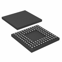
ADUC7122BBCZ-RL Analog Devices Inc, ADUC7122BBCZ-RL Datasheet - Page 73

ADUC7122BBCZ-RL
Manufacturer Part Number
ADUC7122BBCZ-RL
Description
PRECISION ANALOG MCU I.C
Manufacturer
Analog Devices Inc
Series
MicroConverter® ADuC7xxxr
Datasheet
1.ADUC7122BBCZ.pdf
(96 pages)
Specifications of ADUC7122BBCZ-RL
Core Processor
ARM7
Core Size
16/32-Bit
Speed
41.78MHz
Connectivity
I²C, SPI, UART/USART
Peripherals
POR, PWM, WDT
Number Of I /o
32
Program Memory Size
126KB (63K x 16)
Program Memory Type
FLASH
Ram Size
8K x 8
Voltage - Supply (vcc/vdd)
3 V ~ 3.6 V
Data Converters
A/D 13x12b, D/A 12x12b
Oscillator Type
Internal
Operating Temperature
-10°C ~ 95°C
Package / Case
108-LFBGA, CSPBGA
Lead Free Status / RoHS Status
Lead free / RoHS Compliant
Eeprom Size
-
Lead Free Status / RoHS Status
Lead free / RoHS Compliant
Other names
ADUC7122BBCZ-RL
ADUC7122BBCZ-RLTR
ADUC7122BBCZ-RLTR
Available stocks
Company
Part Number
Manufacturer
Quantity
Price
Company:
Part Number:
ADUC7122BBCZ-RL
Manufacturer:
Analog Devices Inc
Quantity:
10 000
PROGRAMMABLE LOGIC ARRAY (PLA)
The ADuC7122 integrates a fully programmable logic array
(PLA) that consists of two, independent but interconnected
PLA blocks. Each block consists of eight PLA elements, giving
each part a total of 16 PLA elements.
Each PLA element contains a two-input look-up table that can
be configured to generate any logic output function based on
two inputs and a flip-flop. This is represented in Figure 35.
In total, 32 GPIO pins are available on each ADuC7122 for the
PLA. These include 16 input pins and 16 output pins that need to
be configured in the GPxCON register as PLA pins before using
the PLA. Note that the comparator output is also included as
one of the 16 input pins.
The PLA is configured via a set of user MMRs. The output(s) of
the PLA can be routed to the internal interrupt system, to the
CONVST signal of the ADC, to an MMR, or to any of the 16
PLA output pins.
The two blocks can be interconnected as follows:
Table 113. Element Input/Output
Element
0
1
2
3
4
5
6
7
Output of Element 15 (Block 1) can be fed back to Input 0 of
Mux 0 of Element 0 (Block 0)
Output of Element 7 (Block 0) can be fed back to the Input 0
of Mux 0 of Element 8 (Block 1)
PLA Block 0
Input
P2.7
P2.2
P0.6
P0.7
P0.1
P0.0
P1.1
P1.0
0
1
2
3
Figure 35. PLA Element
Output
P3.0
P3.1
P3.2
P3.3
P1.7
P1.6
P2.5
P2.4
A
B
LOOKUP
TABLE
Element
8
9
10
11
12
13
14
15
PLA Block 1
Input
P1.4
P1.5
P0.5
P0.4
P2.1
P2.0
P2.3
P2.6
4
Output
P3.4
P3.5
P3.6
P3.7
P0.3
P0.2
P1.3
P1.2
Rev. 0 | Page 73 of 96
PLA MMRs Interface
The PLA peripheral interface consists of the 21 MMRs
described in Table 114 to Table 128.
Table 114. PLAELMx Registers
Name
PLAELM0
PLAELM1
PLAELM2
PLAELM3
PLAELM4
PLAELM5
PLAELM6
PLAELM7
PLAELM8
PLAELM9
PLAELM10
PLAELM11
PLAELM12
PLAELM13
PLAELM14
PLAELM15
PLAELMx are Element 0 to Element 15 control registers. They
configure the input and output mux of each element, select the
function in the look-up table, and bypass/use the flip-flop. See
Table 115 and Table 118.
Address
0xFFFF0B00
0xFFFF0B04
0xFFFF0B08
0xFFFF0B0C
0xFFFF0B10
0xFFFF0B14
0xFFFF0B18
0xFFFF0B1C
0xFFFF0B20
0xFFFF0B24
0xFFFF0B28
0xFFFF0B2C
0xFFFF0B30
0xFFFF0B34
0xFFFF0B38
0xFFFF0B3C
Default Value
0x0000
0x0000
0x0000
0x0000
0x0000
0x0000
0x0000
0x0000
0x0000
0x0000
0x0000
0x0000
0x0000
0x0000
0x0000
0x0000
ADuC7122
Access
R/W
R/W
R/W
R/W
R/W
R/W
R/W
R/W
R/W
R/W
R/W
R/W
R/W
R/W
R/W
R/W


