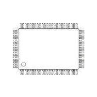
PCA9620H/Q900/1,51 NXP Semiconductors, PCA9620H/Q900/1,51 Datasheet - Page 20

PCA9620H/Q900/1,51
Manufacturer Part Number
PCA9620H/Q900/1,51
Description
LCD Drivers 480 SEGMENT LCD SEGMENT DRIVER
Manufacturer
NXP Semiconductors
Datasheet
1.PCA9620HQ900151.pdf
(71 pages)
Specifications of PCA9620H/Q900/1,51
Number Of Segments
60
Maximum Clock Frequency
14500 Hz
Operating Supply Voltage
2.5 V to 5.5 V
Maximum Power Dissipation
400 mW
Maximum Operating Temperature
+ 105 C
Package / Case
LQFP-80
Maximum Supply Current
200 uA
Minimum Operating Temperature
- 40 C
Lead Free Status / RoHS Status
Lead free / RoHS Compliant
Other names
935291899518
Available stocks
Company
Part Number
Manufacturer
Quantity
Price
Company:
Part Number:
PCA9620H/Q900/1,51
Manufacturer:
NXP Semiconductors
Quantity:
10 000
NXP Semiconductors
PCA9620
Product data sheet
7.4.1 LCD voltage selector
7.4 LCD voltage
Remark: It is necessary to run the power-down sequence before removing the supplies.
Depending on the application, care must be taken that no other signals are present at the
chip input or output pins when removing the supplies (please refer to
page
removal of supply voltages the PCA9620 will not be damaged.
Remark: Static voltages across the liquid crystal display can build up when the external
LCD supply voltage (V
versa. This may cause unwanted display artifacts. To avoid such artifacts, external V
V
Remark: A clock signal must always be supplied to the device when the device is active;
removing the clock may freeze the LCD in a DC state, which is not suitable for the liquid
crystal. It is recommended to first disable the display and afterwards to remove the clock
signal.
The LCD voltage selector co-ordinates the multiplexing of the LCD in accordance with the
selected LCD drive configuration. The operation of the voltage selector is controlled by the
set-bias-mode command (see
(see
Intermediate LCD biasing voltages are obtained from an internal voltage divider. The
biasing configurations that apply to the preferred modes of operation, together with the
biasing characteristics as functions of V
given in
Discrimination is a term which is defined as the ratio of the on and off RMS voltage across
a segment. It can be thought of as a measurement of contrast.
Fig 13. Recommended power-down sequence when using an external supplied V
DD1
, and V
Table 13 on page
53). Otherwise this may cause unwanted display artifacts. In case of uncontrolled
Table
an external clock signal
DD2
26.
All information provided in this document is subject to legal disclaimers.
must be applied or removed together.
Rev. 1 — 9 December 2010
LCD
8).
) is on while the IC supply voltage (V
play by setting
perature mea-
Disable tem-
surement by
bit E logic 0
TME logic 0
Disable dis-
setting bit
Table 14 on page
START
LCD
Universal LCD driver for low multiplex rates
and the resulting discrimination ratios (D), are
8) and the set-MUX-mode command
Bring pin CLK
to 3-state by
OSC and bit
COE logic 0
be switched
setting bit
clock may
External
STOP
off
013aaa256
DD1
or V
Section 9 on
PCA9620
DD2
© NXP B.V. 2010. All rights reserved.
) is off, or vice
LCD
20 of 71
and
LCD
,


