PCA9620H/Q900/1,51 NXP Semiconductors, PCA9620H/Q900/1,51 Datasheet - Page 40
PCA9620H/Q900/1,51
Manufacturer Part Number
PCA9620H/Q900/1,51
Description
LCD Drivers 480 SEGMENT LCD SEGMENT DRIVER
Manufacturer
NXP Semiconductors
Datasheet
1.PCA9620HQ900151.pdf
(71 pages)
Specifications of PCA9620H/Q900/1,51
Number Of Segments
60
Maximum Clock Frequency
14500 Hz
Operating Supply Voltage
2.5 V to 5.5 V
Maximum Power Dissipation
400 mW
Maximum Operating Temperature
+ 105 C
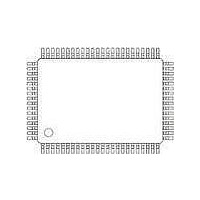
Package / Case
LQFP-80
Maximum Supply Current
200 uA
Minimum Operating Temperature
- 40 C
Lead Free Status / RoHS Status
Lead free / RoHS Compliant
Other names
935291899518
Available stocks
Company
Part Number
Manufacturer
Quantity
Price
Company:

Part Number:
PCA9620H/Q900/1,51
Manufacturer:
NXP Semiconductors
Quantity:
10 000


NXP Semiconductors
PCA9620
Product data sheet
7.7 Segment outputs
7.8 Display register
7.9 Display RAM
The LCD drive section includes 60 segment outputs (S0 to S59) which must be connected
directly to the LCD. The segment output signals are generated based on the multiplexed
backplane signals and with data resident in the display register. When less than
60 segment outputs are required, the unused segment outputs must be left open-circuit.
The display register holds the display data while the corresponding multiplex signals are
generated.
The display RAM is a static 60 × 8-bit RAM which stores LCD data. Logic 1 in the RAM bit
map indicates the on-state of the corresponding LCD element; similarly, logic 0 indicates
the off-state.
There is a one-to-one correspondence between
The display RAM bit map,
backplane outputs BP0 to BP7, and column 0 to column 59 which correspond with the
segment outputs S0 to S59. In multiplexed LCD applications the data of each row of the
display RAM is time-multiplexed with the corresponding backplane (row 0 with BP0, row 1
with BP1 and so on).
When display data is transmitted to the PCA9620 the display bytes received are stored in
the display RAM in accordance with the selected LCD multiplex drive mode. The data is
stored as it arrives and does not wait for the acknowledge cycle as with the commands.
Depending on the current multiplex drive mode, data is stored singularly, in pairs,
quadruples, sextuples or bytes.
•
•
•
the bits in the RAM bitmap and the LCD elements
the RAM columns and the segment outputs
the RAM rows and the backplane outputs.
All information provided in this document is subject to legal disclaimers.
Rev. 1 — 9 December 2010
Figure
30, shows row 0 to row 7 which correspond with the
Universal LCD driver for low multiplex rates
PCA9620
© NXP B.V. 2010. All rights reserved.
40 of 71
Related parts for PCA9620H/Q900/1,51
Image
Part Number
Description
Manufacturer
Datasheet
Request
R

Part Number:
Description:
Universal LCD driver for low multiplex rates
Manufacturer:
NXP [NXP Semiconductors]
Datasheet:

Part Number:
Description:
NXP Semiconductors designed the LPC2420/2460 microcontroller around a 16-bit/32-bitARM7TDMI-S CPU core with real-time debug interfaces that include both JTAG andembedded trace
Manufacturer:
NXP Semiconductors
Datasheet:

Part Number:
Description:
NXP Semiconductors designed the LPC2458 microcontroller around a 16-bit/32-bitARM7TDMI-S CPU core with real-time debug interfaces that include both JTAG andembedded trace
Manufacturer:
NXP Semiconductors
Datasheet:
Part Number:
Description:
NXP Semiconductors designed the LPC2468 microcontroller around a 16-bit/32-bitARM7TDMI-S CPU core with real-time debug interfaces that include both JTAG andembedded trace
Manufacturer:
NXP Semiconductors
Datasheet:
Part Number:
Description:
NXP Semiconductors designed the LPC2470 microcontroller, powered by theARM7TDMI-S core, to be a highly integrated microcontroller for a wide range ofapplications that require advanced communications and high quality graphic displays
Manufacturer:
NXP Semiconductors
Datasheet:
Part Number:
Description:
NXP Semiconductors designed the LPC2478 microcontroller, powered by theARM7TDMI-S core, to be a highly integrated microcontroller for a wide range ofapplications that require advanced communications and high quality graphic displays
Manufacturer:
NXP Semiconductors
Datasheet:
Part Number:
Description:
The Philips Semiconductors XA (eXtended Architecture) family of 16-bit single-chip microcontrollers is powerful enough to easily handle the requirements of high performance embedded applications, yet inexpensive enough to compete in the market for hi
Manufacturer:
NXP Semiconductors
Datasheet:
Part Number:
Description:
The XA-S3 device is a member of Philips Semiconductors? XA(eXtended Architecture) family of high performance 16-bitsingle-chip microcontrollers
Manufacturer:
NXP Semiconductors
Datasheet:

Part Number:
Description:
The NXP BlueStreak LH75401/LH75411 family consists of two low-cost 16/32-bit System-on-Chip (SoC) devices
Manufacturer:
NXP Semiconductors
Datasheet:
Part Number:
Description:
The NXP LPC3130/3131 combine an 180 MHz ARM926EJ-S CPU core, high-speed USB2
Manufacturer:
NXP Semiconductors
Datasheet:
Part Number:
Description:
The NXP LPC3141 combine a 270 MHz ARM926EJ-S CPU core, High-speed USB 2
Manufacturer:
NXP Semiconductors
Part Number:
Description:
The NXP LPC3143 combine a 270 MHz ARM926EJ-S CPU core, High-speed USB 2
Manufacturer:
NXP Semiconductors

Part Number:
Description:
The NXP LPC3152 combines an 180 MHz ARM926EJ-S CPU core, High-speed USB 2
Manufacturer:
NXP Semiconductors