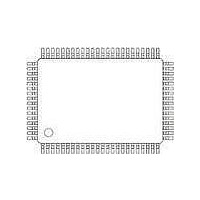
PCA9620H/Q900/1,51 NXP Semiconductors, PCA9620H/Q900/1,51 Datasheet - Page 38

PCA9620H/Q900/1,51
Manufacturer Part Number
PCA9620H/Q900/1,51
Description
LCD Drivers 480 SEGMENT LCD SEGMENT DRIVER
Manufacturer
NXP Semiconductors
Datasheet
1.PCA9620HQ900151.pdf
(71 pages)
Specifications of PCA9620H/Q900/1,51
Number Of Segments
60
Maximum Clock Frequency
14500 Hz
Operating Supply Voltage
2.5 V to 5.5 V
Maximum Power Dissipation
400 mW
Maximum Operating Temperature
+ 105 C
Package / Case
LQFP-80
Maximum Supply Current
200 uA
Minimum Operating Temperature
- 40 C
Lead Free Status / RoHS Status
Lead free / RoHS Compliant
Other names
935291899518
Available stocks
Company
Part Number
Manufacturer
Quantity
Price
Company:
Part Number:
PCA9620H/Q900/1,51
Manufacturer:
NXP Semiconductors
Quantity:
10 000
NXP Semiconductors
PCA9620
Product data sheet
7.5.1 Internal oscillator
7.5.2 External clock
7.5 Oscillator
The V
Table 30.
[1]
Example: Assumed that T
The VT[7:0] term is calculated using the digital temperature value TD[7:0] which is
provided by the temperature measurement block
of the temperature measurement block (T
translated to the LCD voltage deviation ΔV
Since VT[7:0] = f[T,slope] and T
of the possible values specified in
voltage deviation ΔV
be:
The internal logic and LCD drive signals of the PCA9620 are timed by a frequency f
which either is the built-in oscillator frequency f
When the internal oscillator is used, it is possible to make the clock signal available on pin
CLK by using the oscillator-ctrl command (see
pin CLK should be left open. At power-on the signal at pin CLK is disabled and pin CLK is
in 3-state.
The duty cycle of the output clock provided on the CLK pin is not always 50 : 50.
on page 9
In applications where an external clock needs to be applied to the PCA9620, bit OSC (see
Table 7 on page
The CLK signal is a signal that is fed into the V
equal to the V
The clock frequency (f
V
V
30mV
Temperature range
T ≤ −40 °C
−40 °C ≤ T ≤ −10 °C
−10 °C < T ≤ 20 °C
20 °C < T ≤ 50 °C
50 °C < T < 80 °C
80 °C ≤ T
offset LCD
offset LCD
ΔV
No temperature compensation is possible above 80 °C. Above this value, the system maintains the
compensation value from 80 °C.
offset(LCD)
(
(
×
offset LCD
–
30
)
)
shows the expected duty cycle for each of the chosen frame frequencies.
Calculation of the temperature compensated voltage V
(
=
=
×
–
DD1
m
m
value can be calculated with the equations given in
0.5
All information provided in this document is subject to legal disclaimers.
)tot
6) must be set logic 1. In this case pin CLK becomes an input.
×
×
voltage supplied to the chip and be referenced to V
V
V
=
=
T
T
offset(LCD)tot
450mV
Rev. 1 — 9 December 2010
ΔV
=
clk
) determines the LCD frame frequency f
m
LCD
amb
×
TD[7:0]
0h
0h to 20h
21h to 40h
41h to 60h
61h to 7Eh
7Fh
(
+
TD[7:0] 64
= −8 °C; TD[7:0] = 22h; MB = −0.5:
[1]
ΔV
acc
over the temperature range. So the total V
T
= ±6 °C then
Table
.
–
29. This term will be added to the total LCD
acc
)
Universal LCD driver for low multiplex rates
LCD
Offset equation for V
V
V
V
V
V
V
×
T
T
T
T
T
T
, see
MB
.
=
=
=
=
=
=
osc
Table 7 on page
DD1
ΔV
–
(
(
(
(
31 MD
TD 7:0
TD 7:0
TD 7:0
TD 7:0
32
(Section
=
Table 35 on page
or equals an external clock frequency.
T
×
domain so it must have an amplitude
×
[
[
[
[
30mV
=
MA
T
] 32
] 64
] 64
] 96
– (
+
acc
–
–
–
–
32
×
7.4.7). Therefore the accuracy
32 MB
×
(
)
)
)
)
×
(
×
) MB
slope
×
×
×
34 64
MC
×
T
MA 32 MB
MC
MD
6). If this is not intended,
T
fr
–
.
–
Table
+
, where slope has one
55) will be directly
32 MC
)
SS
PCA9620
×
×
© NXP B.V. 2010. All rights reserved.
×
.
–
30:
0.5
LCD
)
=
offset will
Table 17
38 of 71
clk
(12)


