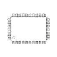
PCA9620H/Q900/1,51 NXP Semiconductors, PCA9620H/Q900/1,51 Datasheet - Page 46

PCA9620H/Q900/1,51
Manufacturer Part Number
PCA9620H/Q900/1,51
Description
LCD Drivers 480 SEGMENT LCD SEGMENT DRIVER
Manufacturer
NXP Semiconductors
Datasheet
1.PCA9620HQ900151.pdf
(71 pages)
Specifications of PCA9620H/Q900/1,51
Number Of Segments
60
Maximum Clock Frequency
14500 Hz
Operating Supply Voltage
2.5 V to 5.5 V
Maximum Power Dissipation
400 mW
Maximum Operating Temperature
+ 105 C
Package / Case
LQFP-80
Maximum Supply Current
200 uA
Minimum Operating Temperature
- 40 C
Lead Free Status / RoHS Status
Lead free / RoHS Compliant
Other names
935291899518
Available stocks
Company
Part Number
Manufacturer
Quantity
Price
Company:
Part Number:
PCA9620H/Q900/1,51
Manufacturer:
NXP Semiconductors
Quantity:
10 000
NXP Semiconductors
PCA9620
Product data sheet
7.9.2 Bank selection
In order to fill the whole RAM addresses 60 bytes need to be sent to the PCA9620. After
the last byte sent the data pointer is wrapped around to column 0 to start a possible RAM
content update (see
transmitted data byte can be written over the RAM boundary.
A RAM bank can be thought of as a collection of RAM rows. The PCA9620 includes a
RAM bank switching feature in the static, 1:2, and 1:4 multiplex drive modes.
The RAM bank switching gives the provision for preparing display information in an
alternative bank and to be able to switch to it once it is complete. Input and output banks
can be set independently from one another with the input-bank-select and the
output-bank-select commands;
Fig 39. Display RAM filling order in 1:8 multiplex drive mode
Fig 40. Data pointer wrap around in 1:8 multiplex drive mode
display RAM rows/
backplane outputs
(BP)
rows
All information provided in this document is subject to legal disclaimers.
display RAM
data pointer
0
1
2
3
4
5
6
7
b7
b6
b5
b4
b3
b2
b1
b0
0
Figure
Rev. 1 — 9 December 2010
1
2
display RAM columns/segment outputs (S)
40). In this case there is no situation possible where a
0
1
2
3
4
5
6
7
3
b7
b6
b5
b4
b3
b2
b1
b0
0
4
Figure 41
1
5
2
6
columns
3
7
4
shows the concept.
Universal LCD driver for low multiplex rates
5
wrap around
6
55 56 57 58 59
7
55 56 57 58 59
MSB
013aaa291
b7
b6
transmitted data byte
a7
a6
a5
a4
a3
a2
a1
a0
PCA9620
b5
© NXP B.V. 2010. All rights reserved.
b4
b3
b2
013aaa267
b1
46 of 71
LSB
b0


