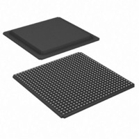
XC3SD3400A-4FGG676C Xilinx Inc, XC3SD3400A-4FGG676C Datasheet - Page 18

XC3SD3400A-4FGG676C
Manufacturer Part Number
XC3SD3400A-4FGG676C
Description
FPGA, SPARTAN-3A, DSP, 676FBGA
Manufacturer
Xilinx Inc
Series
Spartan™-3A DSPr
Datasheets
1.XC3S50A-4VQG100C.pdf
(7 pages)
2.XC3SD3400A-4FGG676C.pdf
(4 pages)
3.XC3SD3400A-4FGG676C.pdf
(101 pages)
Specifications of XC3SD3400A-4FGG676C
No. Of Logic Blocks
5968
No. Of Gates
3400000
No. Of Macrocells
53712
Family Type
Spartan-3A
No. Of Speed Grades
4
Total Ram Bits
2322432
No. Of I/o's
502
Clock Management
DCM
I/o Supply
RoHS Compliant
Number Of Logic Elements/cells
53712
Number Of Labs/clbs
5968
Number Of I /o
469
Number Of Gates
3400000
Voltage - Supply
1.14 V ~ 1.26 V
Mounting Type
Surface Mount
Operating Temperature
0°C ~ 85°C
Package / Case
676-BBGA
Package
676FBGA
Family Name
Spartan®-3A
Device Logic Units
53712
Device System Gates
3400000
Maximum Internal Frequency
667 MHz
Typical Operating Supply Voltage
1.2 V
Maximum Number Of User I/os
469
Ram Bits
2322432
Rohs Compliant
Yes
Lead Free Status / RoHS Status
Lead free / RoHS Compliant
For Use With
122-1532 - KIT DEVELOPMENT SPARTAN 3ADSP
Lead Free Status / RoHS Status
Lead free / RoHS Compliant
Other names
122-1539
Available stocks
Company
Part Number
Manufacturer
Quantity
Price
Company:
Part Number:
XC3SD3400A-4FGG676C
Manufacturer:
XilinxInc
Quantity:
3 000
Company:
Part Number:
XC3SD3400A-4FGG676C
Manufacturer:
Xilinx Inc
Quantity:
10 000
Company:
Part Number:
XC3SD3400A-4FGG676C
Manufacturer:
XILINX
Quantity:
592
Part Number:
XC3SD3400A-4FGG676C
Manufacturer:
XILINX/赛灵思
Quantity:
20 000
External Termination Requirements for Differential I/O
LVDS, RSDS, MINI_LVDS, and PPDS I/O Standards
X-Ref Target - Figure 5
BLVDS_25 I/O Standard
X-Ref Target - Figure 6
TMDS_33 I/O Standard
X-Ref Target - Figure 7
Device DNA Read Endurance
Table 14: Device DNA Identifier Memory Characteristics
DS610 (v3.0) October 4, 2010
Product Specification
DNA_CYCLES
Symbol
Figure 5: External Input Termination for LVDS, RSDS, MINI_LVDS, and PPDS I/O Standards
Figure 6: External Output and Input Termination Resistors for BLVDS_25 I/O Standard
V
V
MINI_LVDS_33,
RSDS_33,
PPDS_33
MINI_LVDS_33,
RSDS_33,
PPDS_33
LVDS_33,
LVDS_33,
CCO
CCO
= 3.3V
= 3.3V
Number of READ operations or JTAG ISC_DNA read operations. Unaffected by
HOLD or SHIFT operations.
Figure 7: External Input Resistors Required for TMDS_33 I/O Standard
V
V
V
Any Bank
MINI_LVDS_25,
RSDS_25,
PPDS_25
MINI_LVDS_25,
RSDS_25,
PPDS_25
LVDS_25,
LVDS_25,
CCO
a) Input-only differential pairs or pairs not using DIFF_TERM=Yes constraint
BLVDS_25
b) Differential pairs using DIFF_TERM=Yes constraint
CCO
CCO
Bank 0
Bank 2
= 2.5V
= 2.5V
= 2.5V
Bank 0 and 2
Bank 0 and 2
V
CCO
TMDS_33
Bank 0
Bank 2
165Ω
165Ω
Bank 0
Bank 2
1 4
CAT16-LV4F12
/ th of Bourns
= 3.3V
Part Number
140Ω
DVI/HDMI cable
Spartan-3A DSP FPGA Family: DC and Switching Characteristics
Description
www.xilinx.com
Z
Z
Z
Z
0
0
0
0
Z
Z
= 50Ω
= 50Ω
= 50Ω
= 50Ω
0
0
50Ω
= 50Ω
= 50Ω
1 4
3.3V
CAT16-PT4F4
/ th of Bourns
Part Number
1 4
CAT16-PT4F4
/ th of Bourns
Part Number
100Ω
50Ω
100Ω
V
DIFF_TERM=No
DIFF_TERM=Yes
Any Bank
TMDS_33
CCAUX
DS529-3_08_020107
Bank 0
Bank 2
Any Bank
BLVDS_25
No V
Any Bank
R
Bank 0
Bank 2
= 3.3V
DT
Bank 0
Bank 2
CCO
V
LVDS_33,
MINI_LVDS_33,
RSDS_33,
PPDS_33
Requirement
CCO
DS529-3_07_020107
No V
LVDS_33, LVDS_25,
MINI_LVDS_33,
MINI_LVDS_25,
RSDS_33, RSDS_25,
PPDS_33, PPDS_25
= 3.3V
CCO
Restrictions
DS529-3_09_020107
V
LVDS_25,
MINI_LVDS_25,
RSDS_25,
PPDS_25
CCO
30,000,000
Minimum
= 2.5V
cycles
Units
Read
18


