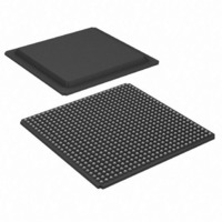
XC3SD3400A-4FGG676C Xilinx Inc, XC3SD3400A-4FGG676C Datasheet - Page 63

XC3SD3400A-4FGG676C
Manufacturer Part Number
XC3SD3400A-4FGG676C
Description
FPGA, SPARTAN-3A, DSP, 676FBGA
Manufacturer
Xilinx Inc
Series
Spartan™-3A DSPr
Datasheets
1.XC3S50A-4VQG100C.pdf
(7 pages)
2.XC3SD3400A-4FGG676C.pdf
(4 pages)
3.XC3SD3400A-4FGG676C.pdf
(101 pages)
Specifications of XC3SD3400A-4FGG676C
No. Of Logic Blocks
5968
No. Of Gates
3400000
No. Of Macrocells
53712
Family Type
Spartan-3A
No. Of Speed Grades
4
Total Ram Bits
2322432
No. Of I/o's
502
Clock Management
DCM
I/o Supply
RoHS Compliant
Number Of Logic Elements/cells
53712
Number Of Labs/clbs
5968
Number Of I /o
469
Number Of Gates
3400000
Voltage - Supply
1.14 V ~ 1.26 V
Mounting Type
Surface Mount
Operating Temperature
0°C ~ 85°C
Package / Case
676-BBGA
Package
676FBGA
Family Name
Spartan®-3A
Device Logic Units
53712
Device System Gates
3400000
Maximum Internal Frequency
667 MHz
Typical Operating Supply Voltage
1.2 V
Maximum Number Of User I/os
469
Ram Bits
2322432
Rohs Compliant
Yes
Lead Free Status / RoHS Status
Lead free / RoHS Compliant
For Use With
122-1532 - KIT DEVELOPMENT SPARTAN 3ADSP
Lead Free Status / RoHS Status
Lead free / RoHS Compliant
Other names
122-1539
Available stocks
Company
Part Number
Manufacturer
Quantity
Price
Company:
Part Number:
XC3SD3400A-4FGG676C
Manufacturer:
XilinxInc
Quantity:
3 000
Company:
Part Number:
XC3SD3400A-4FGG676C
Manufacturer:
Xilinx Inc
Quantity:
10 000
Company:
Part Number:
XC3SD3400A-4FGG676C
Manufacturer:
XILINX
Quantity:
592
Part Number:
XC3SD3400A-4FGG676C
Manufacturer:
XILINX/赛灵思
Quantity:
20 000
Table 57: Types of Pins on Spartan-3A DSP FPGAs (Cont’d)
Package Pins by Type
Each package has three separate voltage supply
inputs—VCCINT, VCCAUX, and VCCO—and a common
ground return, GND. The numbers of pins dedicated to
these functions vary by package, as shown in
Table 58: Power and Ground Supply Pins by Package
A majority of package pins are user-defined I/O or input
pins. However, the numbers and characteristics of these I/O
depend on the device type and the package in which it is
available, as shown in
maximum number of single-ended I/O pins available,
Table 59: Maximum User I/O by Package
DS610 (v3.0) October 4, 2010
Product Specification
Notes:
1.
Notes:
1.
Type/Color
Package
Package
VCCAUX
CS484
FG676
VCCINT
CS484
FG676
MGMT
VCCO
Code
JTAG
PWR
GND
# = I/O bank number, an integer between 0 and 3.
Some VREFs are on INPUT pins. See pinout tables for details.
N.C.
XC3SD1800A
XC3SD3400A
XC3SD1800A
XC3SD3400A
XC3SD1800A
XC3SD3400A
XC3SD1800A
XC3SD3400A
Control and status pins for the power-saving Suspend mode. SUSPEND is a dedicated pin
and is powered by VCCAUX. AWAKE is a dual-purpose pin. Unless Suspend mode is enabled
in the application, AWAKE is available as a user-I/O pin.
Dedicated JTAG pin - 4 per device. Not available as a user-I/O pin. Every package has four
dedicated JTAG pins. These pins are powered by VCCAUX.
Dedicated ground pin. The number of GND pins depends on the package used. All must be
connected.
Dedicated auxiliary power supply pin. The number of VCCAUX pins depends on the package
used. All must be connected. Set on board and using CONFIG VCCAUX constraint.
Dedicated internal core logic power supply pin. The number of VCCINT pins depends on the
package used. All must be connected to +1.2V.
Along with all the other VCCO pins in the same bank, this pin supplies power to the output
buffers within the I/O bank and sets the input threshold voltage for some I/O standards. All
must be connected.
This package pin is not connected in this specific device/package combination but may be
connected in larger devices in the same package.
Device
Device
Table
VCCINT
User I/Os and
59. The table shows the
Input-Only
36
36
23
36
Maximum
309
309
519
469
VCCAUX VCCO
24
24
14
24
Input-Only
Maximum
Table
110
60
60
60
24
24
36
40
Description
58.
GND
www.xilinx.com
100
84
84
77
Differential
Maximum
Pairs
140
140
227
213
assuming that all I/O-, INPUT-, DUAL-, VREF-, and
CLK-type pins are used as general-purpose I/O. AWAKE is
counted here as a dual-purpose I/O pin. Likewise, the table
shows the maximum number of differential pin-pairs
available on the package. Finally, the table shows how the
total maximum user-I/Os are distributed by pin type,
including the number of unconnected—N.C.—pins on the
device.
Not all I/O standards are supported on all I/O banks. The left
and right banks (I/O banks 1 and 3) support higher output
drive current than the top and bottom banks (I/O banks 0
and 2). Similarly, true differential output standards, such as
LVDS, RSDS, PPDS, miniLVDS, and TMDS, are only
supported in the top or bottom banks (I/O banks 0 and 2).
Inputs are unrestricted. For more details, see the Using I/O
Resources chapter in UG331.
Spartan-3A DSP FPGA Family: Pinout Descriptions
156
156
314
314
I/O
INPUT
41
41
82
34
All Possible I/Os by Type
DUAL
52
52
52
52
VREF
28
28
39
37
SUSPEND, AWAKE
TDI, TMS, TCK, TDO
GND
VCCAUX
VCCINT
VCCO_#
N.C.
Pin Name(s) in Type
(1)
CLK
32
32
32
32
N.C.
0
0
0
0
63


