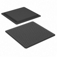
XC3SD3400A-4FGG676C Xilinx Inc, XC3SD3400A-4FGG676C Datasheet - Page 41

XC3SD3400A-4FGG676C
Manufacturer Part Number
XC3SD3400A-4FGG676C
Description
FPGA, SPARTAN-3A, DSP, 676FBGA
Manufacturer
Xilinx Inc
Series
Spartan™-3A DSPr
Datasheets
1.XC3S50A-4VQG100C.pdf
(7 pages)
2.XC3SD3400A-4FGG676C.pdf
(4 pages)
3.XC3SD3400A-4FGG676C.pdf
(101 pages)
Specifications of XC3SD3400A-4FGG676C
No. Of Logic Blocks
5968
No. Of Gates
3400000
No. Of Macrocells
53712
Family Type
Spartan-3A
No. Of Speed Grades
4
Total Ram Bits
2322432
No. Of I/o's
502
Clock Management
DCM
I/o Supply
RoHS Compliant
Number Of Logic Elements/cells
53712
Number Of Labs/clbs
5968
Number Of I /o
469
Number Of Gates
3400000
Voltage - Supply
1.14 V ~ 1.26 V
Mounting Type
Surface Mount
Operating Temperature
0°C ~ 85°C
Package / Case
676-BBGA
Package
676FBGA
Family Name
Spartan®-3A
Device Logic Units
53712
Device System Gates
3400000
Maximum Internal Frequency
667 MHz
Typical Operating Supply Voltage
1.2 V
Maximum Number Of User I/os
469
Ram Bits
2322432
Rohs Compliant
Yes
Lead Free Status / RoHS Status
Lead free / RoHS Compliant
For Use With
122-1532 - KIT DEVELOPMENT SPARTAN 3ADSP
Lead Free Status / RoHS Status
Lead free / RoHS Compliant
Other names
122-1539
Available stocks
Company
Part Number
Manufacturer
Quantity
Price
Company:
Part Number:
XC3SD3400A-4FGG676C
Manufacturer:
XilinxInc
Quantity:
3 000
Company:
Part Number:
XC3SD3400A-4FGG676C
Manufacturer:
Xilinx Inc
Quantity:
10 000
Company:
Part Number:
XC3SD3400A-4FGG676C
Manufacturer:
XILINX
Quantity:
592
Part Number:
XC3SD3400A-4FGG676C
Manufacturer:
XILINX/赛灵思
Quantity:
20 000
Block RAM Timing
Table 33: Block RAM Timing
DS610 (v3.0) October 4, 2010
Product Specification
Notes:
1.
Clock-to-Output Times
T
T
Setup Times
T
T
T
T
T
T
Hold Times
T
T
T
T
T
T
Clock Timing
T
T
Clock Frequency
F
RCKO_DOA_NC
RCKO_DOA
RCCK_ADDR
RDCK_DIB
RCCK_ENB
RCCK_WEB
RCCK_REGCE
RCCK_RST
RCKC_ADDR
RCKC_DIB
RCKC_ENB
RCKC_WEB
RCKC_REGCE
RCKC_RST
BPWH
BPWL
BRAM
Symbol
The numbers in this table are based on the operating conditions set forth in
When reading from block RAM, the delay from the active transition at
the CLK input to data appearing at the DOUT output
Clock CLK to DOUT output (with output register)
Setup time for the ADDR inputs before the active transition at the CLK
input of the block RAM
Setup time for data at the DIN inputs before the active transition at the
CLK input of the block RAM
Setup time for the EN input before the active transition at the CLK input
of the block RAM
Setup time for the WE input before the active transition at the CLK input
of the block RAM
Setup time for the CE input before the active transition at the CLK input
of the block RAM
Setup time for the RST input before the active transition at the CLK
input of the block RAM
Hold time on the ADDR inputs after the active transition at the CLK
input
Hold time on the DIN inputs after the active transition at the CLK input
Hold time on the EN input after the active transition at the CLK input
Hold time on the WE input after the active transition at the CLK input
Hold time on the CE input after the active transition at the CLK input
Hold time on the RST input after the active transition at the CLK input
High pulse width of the CLK signal
Low pulse width of the CLK signal
Block RAM clock frequency
Description
Spartan-3A DSP FPGA Family: DC and Switching Characteristics
www.xilinx.com
Table
7.
0.40
0.29
0.51
0.64
0.34
0.22
0.09
0.09
0.09
0.09
0.09
0.09
1.56
1.56
Min
–
–
0
-5
Speed Grade
Max
2.38
1.24
320
–
–
–
–
–
–
–
–
–
–
–
–
–
–
0.46
0.33
0.60
0.75
0.40
0.25
0.10
0.10
0.10
0.10
0.10
0.10
1.79
1.79
Min
–
–
0
-4
Max
2.80
1.45
280
–
–
–
–
–
–
–
–
–
–
–
–
–
–
Units
MHz
ns
ns
ns
ns
ns
ns
ns
ns
ns
ns
ns
ns
ns
ns
ns
ns
41


