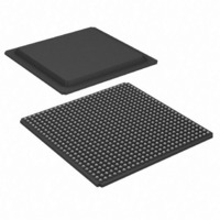
XC3SD3400A-4FGG676C Xilinx Inc, XC3SD3400A-4FGG676C Datasheet - Page 56

XC3SD3400A-4FGG676C
Manufacturer Part Number
XC3SD3400A-4FGG676C
Description
FPGA, SPARTAN-3A, DSP, 676FBGA
Manufacturer
Xilinx Inc
Series
Spartan™-3A DSPr
Datasheets
1.XC3S50A-4VQG100C.pdf
(7 pages)
2.XC3SD3400A-4FGG676C.pdf
(4 pages)
3.XC3SD3400A-4FGG676C.pdf
(101 pages)
Specifications of XC3SD3400A-4FGG676C
No. Of Logic Blocks
5968
No. Of Gates
3400000
No. Of Macrocells
53712
Family Type
Spartan-3A
No. Of Speed Grades
4
Total Ram Bits
2322432
No. Of I/o's
502
Clock Management
DCM
I/o Supply
RoHS Compliant
Number Of Logic Elements/cells
53712
Number Of Labs/clbs
5968
Number Of I /o
469
Number Of Gates
3400000
Voltage - Supply
1.14 V ~ 1.26 V
Mounting Type
Surface Mount
Operating Temperature
0°C ~ 85°C
Package / Case
676-BBGA
Package
676FBGA
Family Name
Spartan®-3A
Device Logic Units
53712
Device System Gates
3400000
Maximum Internal Frequency
667 MHz
Typical Operating Supply Voltage
1.2 V
Maximum Number Of User I/os
469
Ram Bits
2322432
Rohs Compliant
Yes
Lead Free Status / RoHS Status
Lead free / RoHS Compliant
For Use With
122-1532 - KIT DEVELOPMENT SPARTAN 3ADSP
Lead Free Status / RoHS Status
Lead free / RoHS Compliant
Other names
122-1539
Available stocks
Company
Part Number
Manufacturer
Quantity
Price
Company:
Part Number:
XC3SD3400A-4FGG676C
Manufacturer:
XilinxInc
Quantity:
3 000
Company:
Part Number:
XC3SD3400A-4FGG676C
Manufacturer:
Xilinx Inc
Quantity:
10 000
Company:
Part Number:
XC3SD3400A-4FGG676C
Manufacturer:
XILINX
Quantity:
592
Part Number:
XC3SD3400A-4FGG676C
Manufacturer:
XILINX/赛灵思
Quantity:
20 000
Serial Peripheral Interface (SPI) Configuration Timing
X-Ref Target - Figure 13
Table 52: Timing for Serial Peripheral Interface (SPI) Configuration Mode
DS610 (v3.0) October 4, 2010
Product Specification
(Open-Drain)
T
T
T
T
T
T
T
PROG_B
CCLK1
CCLKn
MINIT
INITM
CCO
DCC
CCD
PUDC_B
Symbol
VS[2:0]
CSO_B
INIT_B
M[2:0]
CCLK
(Input)
(Input)
(Input)
(Input)
(Input)
MOSI
DIN
Shaded values indicate specifications on attached SPI Flash PROM.
Initial CCLK clock period
CCLK clock period after FPGA loads ConfigRate setting
Setup time on VS[2:0] variant-select pins and M[2:0] mode pins before the
rising edge of INIT_B
Hold time on VS[2:0] variant-select pins and M[2:0] mode pins after the
rising edge of INIT_B
MOSI output valid delay after CCLK falling edge
Setup time on DIN data input before CCLK rising edge
Hold time on DIN data input after CCLK rising edge
T
MINIT
Figure 13: Waveforms for Serial Peripheral Interface (SPI) Configuration
Pin initially pulled High by internal pull-up resistor if PUDC_B input is Low.
Pin initially high-impedance (Hi-Z) if PUDC_B input is High. External pull-up resistor required on CSO_B.
<1:1:1>
<0:0:1>
PUDC_B must be stable before INIT_B goes High and constant throughout the configuration process.
T
INITM
T
CCLK1
Description
T
CSS
Command
Mode input pins M[2:0] and variant select input pins VS[2:0] are sampled when INIT_B
goes High. After this point, input values do not matter until DONE goes High, at which
point these pins become user-I/O pins.
(msb)
Spartan-3A DSP FPGA Family: DC and Switching Characteristics
T
CCO
www.xilinx.com
T
DSU
T
MCCL1
Command
(msb-1)
T
MCCH1
T
DH
Minimum
Data
50
0
T
T
New ConfigRate active
CCLK1
See
See
See
See
See
MCCL n
Data
T
T
V
Maximum
DCC
Table 46
Table 46
Table 50
Table 50
Table 50
–
–
Data
DS529-3_06_102506
T
T
CCLK n
T
CCD
MCCH n
Units
Data
ns
ns
56


