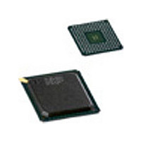
SAA7118E NXP Semiconductors, SAA7118E Datasheet - Page 10

SAA7118E
Manufacturer Part Number
SAA7118E
Description
Manufacturer
NXP Semiconductors
Datasheet
1.SAA7118E.pdf
(177 pages)
Specifications of SAA7118E
Adc/dac Resolution
9b
Screening Level
Commercial
Package Type
LBGA
Pin Count
156
Lead Free Status / RoHS Status
Compliant
Available stocks
Company
Part Number
Manufacturer
Quantity
Price
Part Number:
SAA7118E
Manufacturer:
PHILIPS/飞利浦
Quantity:
20 000
Company:
Part Number:
SAA7118E-V1
Manufacturer:
NXP
Quantity:
5 510
Company:
Part Number:
SAA7118E-V1
Manufacturer:
AD
Quantity:
5 510
Company:
Part Number:
SAA7118E/V1
Manufacturer:
PHI
Quantity:
480
Part Number:
SAA7118E/V1
Manufacturer:
PHILIPS/飞利浦
Quantity:
20 000
Company:
Part Number:
SAA7118E/V1,518
Manufacturer:
NXP Semiconductors
Quantity:
10 000
Company:
Part Number:
SAA7118E/V1,551
Manufacturer:
NXP Semiconductors
Quantity:
10 000
Company:
Part Number:
SAA7118E/V1,557
Manufacturer:
NXP Semiconductors
Quantity:
10 000
Part Number:
SAA7118E/V1/M5
Manufacturer:
PHILIPS/飞利浦
Quantity:
20 000
Company:
Part Number:
SAA7118E/V1/M5,518
Manufacturer:
Sigma Designs Inc
Quantity:
10 000
Company:
Part Number:
SAA7118EH
Manufacturer:
MNDSPEED
Quantity:
335
NXP Semiconductors
Table 4.
SAA7118_7
Product data sheet
Symbol
ADP4
ADP3
V
ADP2
ADP1
ADP0
V
INT_A
V
SCL
V
SDA
RTS0
RTS1
RTCO
AMCLK
V
ASCLK
ALRCLK
AMXCLK
ITRDY
DNC0
DNC16
DNC17
DNC19
DNC20
FSW
ICLK
IDQ
ITRI
DDD3
SSD3
DDD4
SSD4
DDD5
Pin description
Pin
QFP160
57
58
59
60
61
62
63
64
65
66
67
68
69
70
71
72
73
74
75
76
77
78
79
80
81
82
83
84
85
86
LBGA156
P7
L7
M8
M7
P8
N8
L8
P9
M9
N9
L9
P10
M10
N10
L10
P11
M11
N11
P12
M12
N12
P13
N13
N14
-
-
M13
M14
L13
L12
…continued
Type
O
O
P
O
O
O
P
O/od
P
I(/O)
P
I/O/od
O
O
O/st/pd
O
P
O
O/st/pd
I
I/pu
I/pu
NC
NC
NC
NC
I/pd
I/O
O
I(/O)
[1]
Rev. 07 — 7 July 2008
Description
MSB
MSB
digital supply voltage 3 (peripheral cells)
MSB
MSB
LSB of direct analog-to-digital converted output data (VSB)
digital ground 3 (peripheral cells)
I
digital supply voltage 4 (core)
serial clock input (I
digital ground 4 (core)
serial data input/output (I
real-time status or sync information, controlled by subaddresses
11h and 12h; see
real-time status or sync information, controlled by subaddresses
11h and 12h; see
real-time control output; contains information about actual system
clock frequency, field rate, odd/even sequence, decoder status,
subcarrier frequency and phase and PAL sequence (see document
“RTC Functional Description” , available on request); the RTCO pin is
enabled via I
audio master clock output, up to 50 % of crystal clock
digital supply voltage 5 (peripheral cells)
audio serial clock output
audio left/right clock output; can be strapped to supply via a 3.3 k
resistor to indicate that the default 24.576 MHz crystal (pin
ALRCLK = LOW; internal pull-down) has been replaced by a
32.110 MHz crystal (pin ALRCLK = HIGH)
audio master external clock input
target ready input for image port data
do not connect, reserved for future extensions and for testing: scan
input
do not connect, reserved for future extensions and for testing
do not connect, reserved for future extensions and for testing
do not connect, reserved for future extensions and for testing
do not connect, reserved for future extensions and for testing
fast switch (blanking) with internal pull-down inserts component
inputs into CVBS signal
clock output signal for image port, or optional asynchronous
back-end clock input
output data qualifier for image port (optional: gated clock output)
image port output control signal, affects all input port pins inclusive
ICLK, enable and active polarity is under software control (bits IPE in
subaddress 87h); output path used for testing: scan output
2
C-bus interrupt flag (LOW if any enabled status bit has changed)
Multistandard video decoder with adaptive comb filter
4 of direct analog-to-digital converted output data (VSB)
5 of direct analog-to-digital converted output data (VSB)
6 of direct analog-to-digital converted output data (VSB)
7 of direct analog-to-digital converted output data (VSB)
2
C-bus bit RTCE; see
Section 10.2.18
Section 10.2.18
2
C-bus) with inactive output path
2
C-bus)
and
and
Table 35
Section 10.2.19
Section 10.2.19
[2][4]
[2][3]
SAA7118
© NXP B.V. 2008. All rights reserved.
10 of 177


