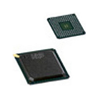
SAA7118E NXP Semiconductors, SAA7118E Datasheet - Page 128

SAA7118E
Manufacturer Part Number
SAA7118E
Description
Manufacturer
NXP Semiconductors
Datasheet
1.SAA7118E.pdf
(177 pages)
Specifications of SAA7118E
Adc/dac Resolution
9b
Screening Level
Commercial
Package Type
LBGA
Pin Count
156
Lead Free Status / RoHS Status
Compliant
Available stocks
Company
Part Number
Manufacturer
Quantity
Price
Part Number:
SAA7118E
Manufacturer:
PHILIPS/飞利浦
Quantity:
20 000
Company:
Part Number:
SAA7118E-V1
Manufacturer:
NXP
Quantity:
5 510
Company:
Part Number:
SAA7118E-V1
Manufacturer:
AD
Quantity:
5 510
Company:
Part Number:
SAA7118E/V1
Manufacturer:
PHI
Quantity:
480
Part Number:
SAA7118E/V1
Manufacturer:
PHILIPS/飞利浦
Quantity:
20 000
Company:
Part Number:
SAA7118E/V1,518
Manufacturer:
NXP Semiconductors
Quantity:
10 000
Company:
Part Number:
SAA7118E/V1,551
Manufacturer:
NXP Semiconductors
Quantity:
10 000
Company:
Part Number:
SAA7118E/V1,557
Manufacturer:
NXP Semiconductors
Quantity:
10 000
Part Number:
SAA7118E/V1/M5
Manufacturer:
PHILIPS/飞利浦
Quantity:
20 000
Company:
Part Number:
SAA7118E/V1/M5,518
Manufacturer:
Sigma Designs Inc
Quantity:
10 000
Company:
Part Number:
SAA7118EH
Manufacturer:
MNDSPEED
Quantity:
335
NXP Semiconductors
Table 93.
[1]
[2]
Table 94.
Table 95.
[1]
Table 96.
SAA7118_7
Product data sheet
I port and scaler back-end clock selection
ICLK output and back-end clock is line-locked clock LLC from decoder
ICLK output and back-end clock is XCLK from X port
ICLK output is LLC and back-end clock is LLC2 clock
Back-end clock is the ICLK input
IDQ pin carries the data qualifier
IDQ pin carries a gated back-end clock (DQ AND CLK)
IDQ generation only for valid data
IDQ qualifies valid data inside the scaling region and all data outside the
scaling region
Output clock phase control
XCLK default output phase, recommended value
XCLK output inverted
XCLK phase shifted by approximately 3 ns
XCLK output inverted and shifted by approximately 3 ns
X port I/O enable
X port output is disabled by software
X port output is enabled by software
X port output is enabled by pin XTRI at logic 0
X port output is enabled by pin XTRI at logic 1
XRDY output signal is A/B task flag from event handler (A = 1)
XRDY output signal is ready signal from scaler path (XRDY = 1 means
the SAA7118 is ready to receive data)
I port signal definitions
IGP0 is output field ID, as defined by OFIDC[90h[6]]
IGP0 is A/B task flag, as defined by CONLH[90h[7]]
IGP0 is sliced data flag, framing the sliced VBI data at the I port
X = don’t care.
Although the ICLK I/O is independent of ICKS2 and ICKS3, this selection can only be used if ICKS2 = 1.
X = don’t care.
Global control 1; global set 80h[3:0]
X port I/O enable and output clock phase control; global set 83h[5:4]
X port I/O enable and output clock phase control; global set 83h[2:0]
I port signal definitions; global set 84h[7:6] and 86h[5]
10.7.2 Subaddresses 83h to 87h
[1]
Rev. 07 — 7 July 2008
Multistandard video decoder with adaptive comb filter
Control bits D3 to D0
ICKS3
X
X
X
X
X
X
0
1
Control bits D5 and D4
XPCK1
0
0
1
1
Control bits D2 to D0
XRQT
X
X
X
X
0
1
Control bits
86h[5]
IDG02
0
0
0
[1]
ICKS2
X
X
X
X
0
1
X
X
[2]
XPE1
0
0
1
1
X
X
84h[7:6]
IDG01
0
0
1
ICKS1
0
0
1
1
X
X
X
X
XPCK0
0
1
0
1
SAA7118
© NXP B.V. 2008. All rights reserved.
XPE0
0
1
0
1
X
X
IDG00
0
1
0
ICKS0
0
1
0
1
X
X
X
X
128 of 177


