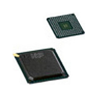
SAA7118E NXP Semiconductors, SAA7118E Datasheet - Page 149

SAA7118E
Manufacturer Part Number
SAA7118E
Description
Manufacturer
NXP Semiconductors
Datasheet
1.SAA7118E.pdf
(177 pages)
Specifications of SAA7118E
Adc/dac Resolution
9b
Screening Level
Commercial
Package Type
LBGA
Pin Count
156
Lead Free Status / RoHS Status
Compliant
Available stocks
Company
Part Number
Manufacturer
Quantity
Price
Part Number:
SAA7118E
Manufacturer:
PHILIPS/飞利浦
Quantity:
20 000
Company:
Part Number:
SAA7118E-V1
Manufacturer:
NXP
Quantity:
5 510
Company:
Part Number:
SAA7118E-V1
Manufacturer:
AD
Quantity:
5 510
Company:
Part Number:
SAA7118E/V1
Manufacturer:
PHI
Quantity:
480
Part Number:
SAA7118E/V1
Manufacturer:
PHILIPS/飞利浦
Quantity:
20 000
Company:
Part Number:
SAA7118E/V1,518
Manufacturer:
NXP Semiconductors
Quantity:
10 000
Company:
Part Number:
SAA7118E/V1,551
Manufacturer:
NXP Semiconductors
Quantity:
10 000
Company:
Part Number:
SAA7118E/V1,557
Manufacturer:
NXP Semiconductors
Quantity:
10 000
Part Number:
SAA7118E/V1/M5
Manufacturer:
PHILIPS/飞利浦
Quantity:
20 000
Company:
Part Number:
SAA7118E/V1/M5,518
Manufacturer:
Sigma Designs Inc
Quantity:
10 000
Company:
Part Number:
SAA7118EH
Manufacturer:
MNDSPEED
Quantity:
335
NXP Semiconductors
12. Limiting values
13. Thermal characteristics
SAA7118_7
Product data sheet
Table 145. Limiting values
In accordance with the Absolute Maximum Rating System (IEC 60134). All ground pins connected
together and grounded (0 V); all supply pins connected together.
[1]
[2]
[3]
Table 146. Thermal characteristics
[1]
Symbol Parameter
V
V
V
V
V
T
T
V
Symbol
R
V
stg
amb
DDD
DDA
i(A)
i(n)
i(D)
esd
th(j-a)
SS
Condition for maximum voltage at digital inputs or I/O pins: 3.0 V < V
Class 2 according to JESD22-A114-B.
Class A according to EIA/JESD22-A115-A.
The overall R
and ground pins must be connected to the power and ground layers directly. An ample copper area directly
under the SAA7118 with a number of through-hole plating, connected to the ground layer (four-layer board:
second layer), can also reduce the effective R
chip. In addition the usage of soldering glue with a high thermal conductance after curing is recommended.
digital supply voltage
analog supply voltage
input voltage at analog inputs
input voltage at pins XTALI, SDA
and SCL
input voltage at digital inputs or
I/O pins
voltage difference between
V
storage temperature
ambient temperature
electrostatic discharge voltage
SSA(n)
Parameter
thermal resistance from junction to
ambient
th(j-a)
SAA7118E
SAA7118H
and V
value can vary depending on the board layout. To minimize the effective R
SSD(n)
Rev. 07 — 7 July 2008
Multistandard video decoder with adaptive comb filter
Conditions
outputs in 3-state
outputs in 3-state
human body model
machine model
th(j-a)
. Please do not use any solder-stop varnish under the
Conditions
in free air
in free air
DDD
[1]
[2]
[3]
< 3.6 V.
[1]
[1]
Min
-
0
-
-
0.5
0.5
0.5
0.5
0.5
0.5
65
Typ
38
29
SAA7118
© NXP B.V. 2008. All rights reserved.
Max
+4.6
+4.6
+4.6
V
+4.6
+5.5
100
+150
70
2000
150
DDD
+ 0.5 V
th(j-a)
Unit
K/W
K/W
149 of 177
all power
Unit
V
V
V
V
V
mV
V
V
C
C


