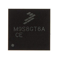
MC9S08GT60ACFDE Freescale, MC9S08GT60ACFDE Datasheet - Page 177

MC9S08GT60ACFDE
Manufacturer Part Number
MC9S08GT60ACFDE
Description
Manufacturer
Freescale
Datasheet
1.MC9S08GT60ACFDE.pdf
(302 pages)
Specifications of MC9S08GT60ACFDE
Cpu Family
HCS08
Device Core Size
8b
Frequency (max)
40MHz
Interface Type
I2C/SCI/SPI
Total Internal Ram Size
4KB
# I/os (max)
39
Number Of Timers - General Purpose
4
Operating Supply Voltage (typ)
2.5/3.3V
Operating Supply Voltage (max)
3.6V
Operating Supply Voltage (min)
1.8/2.08V
On-chip Adc
8-chx10-bit
Instruction Set Architecture
CISC
Operating Temp Range
-40C to 85C
Operating Temperature Classification
Industrial
Mounting
Surface Mount
Pin Count
48
Package Type
QFN EP
Program Memory Type
Flash
Program Memory Size
60KB
Lead Free Status / RoHS Status
Compliant
Available stocks
Company
Part Number
Manufacturer
Quantity
Price
- Current page: 177 of 302
- Download datasheet (8Mb)
11.2.2
This read/write register is used to control various optional features of the SCI system.
Freescale Semiconductor
SCISWAI
Reset
LOOPS
WAKE
RSRC
Field
ILT
PE
PT
M
7
6
5
4
3
2
1
0
W
R
LOOPS
SCI Control Register 1 (SCIxC1)
Loop Mode Select — Selects between loop back modes and normal 2-pin full-duplex modes. When LOOPS = 1,
the transmitter output is internally connected to the receiver input.
0 Normal operation — RxD and TxD use separate pins.
1 Loop mode or single-wire mode where transmitter outputs are internally connected to receiver input. (See
SCI Stops in Wait Mode
0 SCI clocks continue to run in wait mode so the SCI can be the source of an interrupt that wakes up the CPU.
1 SCI clocks freeze while CPU is in wait mode.
Receiver Source Select — This bit has no meaning or effect unless the LOOPS bit is set to 1. When
LOOPS = 1, the receiver input is internally connected to the TxD pin and RSRC determines whether this
connection is also connected to the transmitter output.
0 Provided LOOPS = 1, RSRC = 0 selects internal loop back mode and the SCI does not use the RxD pins.
1 Single-wire SCI mode where the TxD pin is connected to the transmitter output and receiver input.
9-Bit or 8-Bit Mode Select
0 Normal — start + 8 data bits (LSB first) + stop.
1 Receiver and transmitter use 9-bit data characters
Receiver Wakeup Method Select — Refer to
information.
0 Idle-line wakeup.
1 Address-mark wakeup.
Idle Line Type Select — Setting this bit to 1 ensures that the stop bit and logic 1 bits at the end of a character
do not count toward the 10 or 11 bit times of the logic high level by the idle line detection logic. Refer to
Section 11.3.3.2.1, “Idle-Line
0 Idle character bit count starts after start bit.
1 Idle character bit count starts after stop bit.
Parity Enable — Enables hardware parity generation and checking. When parity is enabled, the most significant
bit (MSB) of the data character (eighth or ninth data bit) is treated as the parity bit.
0 No hardware parity generation or checking.
1 Parity enabled.
Parity Type — Provided parity is enabled (PE = 1), this bit selects even or odd parity. Odd parity means the total
number of 1s in the data character, including the parity bit, is odd. Even parity means the total number of 1s in
the data character, including the parity bit, is even.
0 Even parity.
1 Odd parity.
0
7
RSRC
start + 8 data bits (LSB first) + 9th data bit + stop.
bit.) RxD pin is not used by SCI.
SCISWAI
0
6
Table 11-3. SCIxC1 Register Field Descriptions
Figure 11-6. SCI Control Register 1 (SCIxC1)
RSRC
Wakeup” for more information.
MC9S08GB60A Data Sheet, Rev. 2
0
5
M
0
4
Section 11.3.3.2, “Receiver Wakeup
Description
WAKE
3
0
Serial Communications Interface (S08SCIV1)
ILT
0
2
Operation” for more
PE
0
1
PT
0
0
177
Related parts for MC9S08GT60ACFDE
Image
Part Number
Description
Manufacturer
Datasheet
Request
R

Part Number:
Description:
TOWER ELEVATOR BOARDS HARDWARE
Manufacturer:
Freescale Semiconductor
Datasheet:

Part Number:
Description:
TOWER SERIAL I/O HARDWARE
Manufacturer:
Freescale Semiconductor
Datasheet:

Part Number:
Description:
LCD MODULE FOR TWR SYSTEM
Manufacturer:
Freescale Semiconductor
Datasheet:

Part Number:
Description:
DAUGHTER LCD WVGA I.MX51
Manufacturer:
Freescale Semiconductor
Datasheet:

Part Number:
Description:
TOWER SYSTEM BOARD MPC5125
Manufacturer:
Freescale Semiconductor
Datasheet:

Part Number:
Description:
KIT EVALUATION I.MX51
Manufacturer:
Freescale Semiconductor
Datasheet:

Part Number:
Description:
KIT DEVELOPMENT WINCE IMX25
Manufacturer:
Freescale Semiconductor
Datasheet:

Part Number:
Description:
TOWER SYSTEM KIT MPC5125
Manufacturer:
Freescale Semiconductor
Datasheet:

Part Number:
Description:
TOWER SYSTEM BOARD K40X256
Manufacturer:
Freescale Semiconductor
Datasheet:

Part Number:
Description:
TOWER SYSTEM KIT K40X256
Manufacturer:
Freescale Semiconductor
Datasheet:

Part Number:
Description:
Microcontrollers (MCU) MX28 PLATFORM DEV KIT
Manufacturer:
Freescale Semiconductor
Datasheet:

Part Number:
Description:
MCU, MPU & DSP Development Tools IAR KickStart Kit for Kinetis K60
Manufacturer:
Freescale Semiconductor
Datasheet:

Part Number:
Description:
24BIT HDMI MX535/08
Manufacturer:
Freescale Semiconductor
Datasheet:
Part Number:
Description:
Manufacturer:
Freescale Semiconductor, Inc
Datasheet:
Part Number:
Description:
Manufacturer:
Freescale Semiconductor, Inc
Datasheet:


