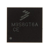
MC9S08GT60ACFDE Freescale, MC9S08GT60ACFDE Datasheet - Page 264

MC9S08GT60ACFDE
Manufacturer Part Number
MC9S08GT60ACFDE
Description
Manufacturer
Freescale
Datasheet
1.MC9S08GT60ACFDE.pdf
(302 pages)
Specifications of MC9S08GT60ACFDE
Cpu Family
HCS08
Device Core Size
8b
Frequency (max)
40MHz
Interface Type
I2C/SCI/SPI
Total Internal Ram Size
4KB
# I/os (max)
39
Number Of Timers - General Purpose
4
Operating Supply Voltage (typ)
2.5/3.3V
Operating Supply Voltage (max)
3.6V
Operating Supply Voltage (min)
1.8/2.08V
On-chip Adc
8-chx10-bit
Instruction Set Architecture
CISC
Operating Temp Range
-40C to 85C
Operating Temperature Classification
Industrial
Mounting
Surface Mount
Pin Count
48
Package Type
QFN EP
Program Memory Type
Flash
Program Memory Size
60KB
Lead Free Status / RoHS Status
Compliant
Available stocks
Company
Part Number
Manufacturer
Quantity
Price
- Current page: 264 of 302
- Download datasheet (8Mb)
Appendix A Electrical Characteristics
264
Low-voltage warning threshold — low range
Power on reset (POR) re-arm voltage
Input high voltage (V
Input high voltage (1.8 V ≤ V
Input low voltage (V
Input low voltage (1.8 V ≤ V
Input hysteresis (all digital inputs)
Input leakage current (per pin)
High impedance (off-state) leakage current (per
pin)
Internal pullup and pulldown resistors
Internal pulldown resistors (Port A4–A7 and IRQ)
Output high voltage (V
Output high voltage (ports C and F)
Maximum total I
Output low voltage (V
Output low voltage (ports C and F)
Maximum total I
Mode = stop
Mode = run and Wait
(all digital inputs)
(all digital inputs)
(all port pins and IRQ)
I
I
I
I
I
I
I
OH
OH
OH
OL
OL
OL
V
V
I
OL
OH
In
In
= 2.0 mA (ports A, B, D, E, and G)
= 6 mA (V
= 3 mA (V
= –10 mA (V
= –6 mA (V
= –3 mA (V
= 10.0 mA (V
= V
= V
= –2 mA (ports A, B, D, E, and G)
DD
DD
or V
or V
OH
OL
DD
DD
SS
SS,
DD
DD
for all port pins
for all port pins
≥ 2.3 V)
≥ 1.8 V)
DD
DD
, all input/output
DD
Parameter
DD
all input only pins
≥ 2.3 V)
DD
≥ 1.8 V)
DD
≥ 2.7 V)
> 2.3 V) (all digital inputs)
≥ 2.7 V)
> 2.3 V) (all digital inputs)
≥ 1.8 V)
≥ 1.8 V)
DD
DD
≤ 2.3 V)
≤ 2.3 V)
(Temperature Range = –40 to 85°C Ambient)
Table A-4. DC Characteristics (Sheet 2 of 3)
(V
(V
(2)
3
DD
DD
falling)
rising)
MC9S08GB60A Data Sheet, Rev. 2
Symbol
V
V
|I
V
|I
Rearm
R
R
V
I
V
LVWL
V
V
|I
OHT
V
V
OLT
OZ
OH
hys
OL
In
PU
PD
IH
IH
IL
IL
|
|
|
0.70 × V
0.85 × V
0.06 × V
V
V
DD
DD
2.08
2.16
0.20
0.50
17.5
17.5
Min
—
—
—
—
—
—
—
—
—
—
– 0.5
– 0.5
DD
DD
DD
Typical
0.025
0.025
2.19
0.30
0.80
2.1
1
0.35 × V
0.30 × V
Freescale Semiconductor
Max
2.27
0.40
52.5
52.5
2.2
1.2
1.0
1.0
0.5
0.5
0.5
0.5
60
60
—
—
—
—
—
—
—
DD
DD
Unit
mA
mA
μA
μA
kΩ
kΩ
V
V
V
V
V
V
V
V
V
Related parts for MC9S08GT60ACFDE
Image
Part Number
Description
Manufacturer
Datasheet
Request
R

Part Number:
Description:
TOWER ELEVATOR BOARDS HARDWARE
Manufacturer:
Freescale Semiconductor
Datasheet:

Part Number:
Description:
TOWER SERIAL I/O HARDWARE
Manufacturer:
Freescale Semiconductor
Datasheet:

Part Number:
Description:
LCD MODULE FOR TWR SYSTEM
Manufacturer:
Freescale Semiconductor
Datasheet:

Part Number:
Description:
DAUGHTER LCD WVGA I.MX51
Manufacturer:
Freescale Semiconductor
Datasheet:

Part Number:
Description:
TOWER SYSTEM BOARD MPC5125
Manufacturer:
Freescale Semiconductor
Datasheet:

Part Number:
Description:
KIT EVALUATION I.MX51
Manufacturer:
Freescale Semiconductor
Datasheet:

Part Number:
Description:
KIT DEVELOPMENT WINCE IMX25
Manufacturer:
Freescale Semiconductor
Datasheet:

Part Number:
Description:
TOWER SYSTEM KIT MPC5125
Manufacturer:
Freescale Semiconductor
Datasheet:

Part Number:
Description:
TOWER SYSTEM BOARD K40X256
Manufacturer:
Freescale Semiconductor
Datasheet:

Part Number:
Description:
TOWER SYSTEM KIT K40X256
Manufacturer:
Freescale Semiconductor
Datasheet:

Part Number:
Description:
Microcontrollers (MCU) MX28 PLATFORM DEV KIT
Manufacturer:
Freescale Semiconductor
Datasheet:

Part Number:
Description:
MCU, MPU & DSP Development Tools IAR KickStart Kit for Kinetis K60
Manufacturer:
Freescale Semiconductor
Datasheet:

Part Number:
Description:
24BIT HDMI MX535/08
Manufacturer:
Freescale Semiconductor
Datasheet:
Part Number:
Description:
Manufacturer:
Freescale Semiconductor, Inc
Datasheet:
Part Number:
Description:
Manufacturer:
Freescale Semiconductor, Inc
Datasheet:


