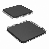
LM9830VJD/NOPB National Semiconductor, LM9830VJD/NOPB Datasheet - Page 19

LM9830VJD/NOPB
Manufacturer Part Number
LM9830VJD/NOPB
Description
IC SCANNER COLOR DOC 100-TQFP
Manufacturer
National Semiconductor
Datasheet
1.LM9830VJDNOPB.pdf
(45 pages)
Specifications of LM9830VJD/NOPB
Number Of Bits
12
Number Of Channels
3
Power (watts)
350mW
Voltage - Supply, Analog
5V
Voltage - Supply, Digital
4.5 V ~ 5.5 V
Package / Case
100-TQFP, 100-VQFP
Lead Free Status / RoHS Status
Lead free / RoHS Compliant
Other names
*LM9830VJD
*LM9830VJD/NOPB
LM9830VJD
*LM9830VJD/NOPB
LM9830VJD
Available stocks
Company
Part Number
Manufacturer
Quantity
Price
Company:
Part Number:
LM9830VJD/NOPB
Manufacturer:
Texas Instruments
Quantity:
10 000
Address
DIGITAL PIXEL RATE OFFSET AND GAIN SETTINGS
PARALLEL PORT SETTINGS
EXTERNAL SRAM SETTINGS
3E
3F
40
41
42
43
Multiplier Gain Range
Smaller gain ranges provide finer control.
Larger gain ranges correct for larger shading
errors.
Offset/Gain data format
Multiplier Coefficient Source
Offset Coefficient Source
Fixed Offset Coefficient
Fixed Multiplier Coefficient - MSB
Fixed Multiplier Coefficient - LSB
Communication Mode
(for reading data from any of the LM9830’s
registers)
Note: This register must be set
appropriately before data can be read
from the LM9830!
Parallel Port Output Driver Current
(I
and fall times into the load capacitance:
rise/fall time approximately equals 5V*C/i)
External SRAM Size
SRAM Interface Output Driver Current
(I
and fall times into the load capacitance:
rise/fall time approximately equals 5V*C/i)
SRAM Bandwidth (8 Bit Data Mode)
8 slot mode should always be used to
maximize performance. If the external
SRAM is to slow to meet the t
requirement, the slower 4 SRAM
accesses/ADC clock mode may be used.
Scanning Duplex (10/12 bit Data Mode)
Full Duplex mode should always be used to
maximize scan speed. If the external SRAM
is to slow to meet the t
the slower Half Duplex mode may be used.
OL
OL
and I
and I
OH
OH
can be used to calculate rise
can be used to calculate rise
Function
RD SETUP
RD SETUP
requirement,
D
n n n n n n n n
n n n n n n n n
7
D
6
D
5
0
1
19
D
0
1
0
1
4
D
0
1
0 0
0 1
1 0
1 1
3
D
2
0
1
0 0
0 1
1 0
1 1
D
1
0 0 1.5:1 (33%)
0 1 2.0:1 (50%)
1 0 3.0:1 (66%)
1 1 Bypass Multiplier
n n Fixed Gain to use for calibration - 2LSBs are assumed
0 0 64 kbytes (not recommended for 600dpi scanners)
0 1 128 kbytes
1 0 256 kbytes
1 1 N/A
D
0 8 bit Bidirectional/EPP
1 4 bit Nibble
0
6 bits offset/10 bits gain
8 bits offset/8 bits gain
Configuration Register 3F (Fixed)
External SRAM
Configuration Register 40 and 41 (Fixed)
External SRAM
Fixed Offset to use for calibration - 2MSBs are
assumed to be 0 if using 6 bit offset format
to be 0 if using 8 bit gain format
I
I
I
I
I
I
I
I
4 SRAM accesses/ADC clock
8 SRAM accesses/ADC clock
(f
Full Duplex- Can transmit data while scanning
(f
Half Duplex - Can only transmit data when buffer is full
or scan has been stopped
OL
OL
OL
OL
OL
OL
OL
OL
MCLK
MCLK
= 5mA, I
= 7mA, I
= 9mA, I
= 15mA, I
= 3.5mA, I
= 6mA, I
= 12mA, I
= 21mA, I
must be 25MHz or lower)
must be 25MHz or lower)
OH
OH
OH
OH
OH
OH
OH
OH
= -6mA
= -9mA
= -12mA
= -7.5mA
= -21mA
= -17mA
= -32mA
= -4mA
Value
http://www.national.com


