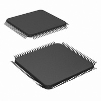
LM9830VJD/NOPB National Semiconductor, LM9830VJD/NOPB Datasheet - Page 34

LM9830VJD/NOPB
Manufacturer Part Number
LM9830VJD/NOPB
Description
IC SCANNER COLOR DOC 100-TQFP
Manufacturer
National Semiconductor
Datasheet
1.LM9830VJDNOPB.pdf
(45 pages)
Specifications of LM9830VJD/NOPB
Number Of Bits
12
Number Of Channels
3
Power (watts)
350mW
Voltage - Supply, Analog
5V
Voltage - Supply, Digital
4.5 V ~ 5.5 V
Package / Case
100-TQFP, 100-VQFP
Lead Free Status / RoHS Status
Lead free / RoHS Compliant
Other names
*LM9830VJD
*LM9830VJD/NOPB
LM9830VJD
*LM9830VJD/NOPB
LM9830VJD
Available stocks
Company
Part Number
Manufacturer
Quantity
Price
Company:
Part Number:
LM9830VJD/NOPB
Manufacturer:
Texas Instruments
Quantity:
10 000
data lines and 9 signaling lines. Additionally, the parallel port
passthrough function requires another set of the 9 control signals.
The LM9830 databus and control signals are tied to the PC’s par-
allel port. To support a parallel port passthrough function, the
LM9830’s control outputs are tri-stated to allow the printer to
communicate with the PC when in passthrough mode. When the
LM9830 is active, the printer is disabled by tri-stating all control
I/O between the printer and the LM9830/PC control bus. A more
detailed description of the parallel port passthrough function is
provided on the full page drawing labelled Printer Passthrough
Block Diagram near the end of this document.
To minimize EMI and on-chip noise, the Parallel Port output driv-
ers (D0-D7 and the 9 control/status output signals) have four out-
put current settings, 0-3. The output current level is set by bits 1
and 2 of Configuration Register 42.
For maximum compatibility and reliability, the “3” setting is recom-
mended. “0” - “2” can be used to reduce EMI and on-chip noise if
the final system (customer’s PC and associated peripherals and
cables) can tolerate it.
D0-D7
STROBE
AUTOFEED
INIT
SELECT IN
ACK
BUSY
PE
SELECT
ERROR
TRISTATE
LATCH
Computer
To
Current
Setting
Name
Figure 50: Printer Passthrough Overview
0
1
2
3
Figure 49: Printer Port Pin Description
Printer Passthrough Signals
Signals
Control
(mA)
Parallel Port Databus
I
To External Buffer
PC Control Signals
To External Latch
9
15
OL
5
7
9
From (To) PC
Direction
From PC
From PC
From PC
From PC
To PC
To PC
To PC
To PC
To PC
(mA)
Databus
I
-12
-21
OH
-6
-9
LM9830
8
200pF
t
F
Passthrough
200
143
111
Buffer
67
(ns)
2
Control
Signals
LM9830
Default
TriState
Input
Input
Input
Input
High
High
Low
Low
Low
Low
Low
t
200pF
R
167
111
83
48
(ns)
Printer
To
34
6.2 Finding the LM9830
The LM9830 powers up in the Transparent mode. In order to com-
municate with the LM9830, the host must send a specific
sequence of data on the databus without changing any of the 4
control signal lines. The LM9830 looks for the sequence 99 66
CC 33 on D0-D7.
Each state (99, 66, CC, and 33) must be held for a minimum of 4
MCLK cycles. After a power on reset status, the MCLK divider is
set to divide-by 4. This means that each state must be held for 16
CRYSTAL IN cycles. For a 50MHz external clock, this means that
each state must be held for a minimum of 16*20ns = 320ns. If the
MCLK divider is programmed to a different value and the LM9830
goes transparent, the minimum time required to wake up the
LM9830 will change. The equation for the length of time each
state must be held is:
The assumption is that this sequence will not occur at random
without any of the 4 control pins violating their static requirement
(STROBE high, the other three static).
When in the transparent mode with a clock applied, the LM9830
constantly monitors the databus for a transition to 99. If 99 is
detected, the LM9830 looks for 66. If 66 is detected, the LM9830
looks for CC. If CC is detected, the LM9830 looks for 33.
If 33 is detected, the LM9830 exits transparent mode.
When the LM9830 exits the Transparent mode it takes the
TRISTATE pin high to disconnect the printer control signals to the
PC, and the LATCH signal low to latch and hold the current state
of the four control signals going to the printer. The 5 control lines
going back to the host change to their deasserted states:
ERROR = high
ACK = high
BUSY = low
PE = low
SELECT = low
At this point the LM9830 software driver can attempt to write to
and read from the configuration register to confirm the pres-
ence/non-presence of the LM9830. Please note that register 42
must be written correctly to allow the LM9830 to respond in the
desired communication mode (8 bit or nibble).
6.3 Selecting EPP or Nibble Mode I/O
Now that the LM9830 has been detected, the Host can start talk-
ing to it. The host PC always writes to the LM9830 using 8 bit
words. For reading data, the LM9830 can communicate in either
8 bit (Bidirectional or EPP) or 4 bit (Nibble) modes, as determined
by the state of register 42, bit 0. This bit has no power-on default
and must be set to a 0 or a 1 before data can be read from the
LM9830.
6.4 Returning to Transparency Mode Without LM9830 Reset
The host can return the LM9830 to Transparency Mode by taking
the INIT pin low and then high again. Approximately 2 - 3 MCLKs
after the rising edge of INIT, the LATCH pin will go high, the
TRISTATE pin will go low, and the LM9830 will tristate its D0-D7
and control line outputs. This will make the LM9830 transparent,
but will not change its operation state. If it was scanning, idling, or
fast feeding, the LM9830 will continue scanning, idling, or fast
t = 4(t
CLK_IN
)(MCLK_DIVIDER)
http://www.national.com


