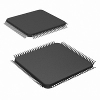
LM9830VJD/NOPB National Semiconductor, LM9830VJD/NOPB Datasheet - Page 29

LM9830VJD/NOPB
Manufacturer Part Number
LM9830VJD/NOPB
Description
IC SCANNER COLOR DOC 100-TQFP
Manufacturer
National Semiconductor
Datasheet
1.LM9830VJDNOPB.pdf
(45 pages)
Specifications of LM9830VJD/NOPB
Number Of Bits
12
Number Of Channels
3
Power (watts)
350mW
Voltage - Supply, Analog
5V
Voltage - Supply, Digital
4.5 V ~ 5.5 V
Package / Case
100-TQFP, 100-VQFP
Lead Free Status / RoHS Status
Lead free / RoHS Compliant
Other names
*LM9830VJD
*LM9830VJD/NOPB
LM9830VJD
*LM9830VJD/NOPB
LM9830VJD
Available stocks
Company
Part Number
Manufacturer
Quantity
Price
Company:
Part Number:
LM9830VJD/NOPB
Manufacturer:
Texas Instruments
Quantity:
10 000
timing is shown in Figure 29, and in slightly more detail in Figure
41.
Illumination Mode 3 is similar to Illumination Mode 2, except that
the LAMP outputs for all three colors are turned on and off every
line. Illumination Mode 3 timing is shown in Figures 30 and 31.
These modes are in operation whenever the chip is powered on
and not in standby mode. For example, the LAMP outputs in Fig-
ures 29 and 30 keep pulsing whether the LM9830 is in the Idle,
Paper Feed, or Scanning states. This eliminates light amplitude
variations due to the lamp/LEDs warm-up characteristics. Since
the LAMP pulses are synchronized to the TR pulse, which is
determined by the horizontal pixel counter, this means that the
pixel counter is constantly running, and any new scans can only
be started by waiting for the next new line (the next Red line in the
case of Illumination Mode 2).
4.2 CCD/CIS Control Block
This function generates the clock signals necessary to control a
CCD or CIS sensor. The LM9830 features:
• Independent control over the polarity (inverting or noninverting)
• Ability to turn off CDS. When CDS is on, traditional CDS is per-
LAMP
LAMP
LAMP
LAMP
LAMP
LAMP
LAMP
LAMP
LAMP
of the input stage to accommodate CIS or CDS signals.
formed. When CDS is off, the signal is sampled at the Sample
Signal point, but the internal reference is used for the Sample
TR
TR
TR
R
G
R
G
G
B
B
R
B
(LAMP
(LAMP
Figure 31: Illumination Mode 3 (green only)
Figure 30: Illumination Mode 3 (grayscale)
Figure 29: Illumination Mode 2
R
B
On > Line End, LAMP
On > Line End, LAMP
B
R
Off < Line End
Off < Line End
29
• The CP1 output supplies the CP pulse needed on some popu-
• A CP2 output is another independent pixel rate pulse that (if
• CCD clock signals RS, CP1, CP2 are reset when Line Ends
• The internal Clamp signal is reset with Optical Black Pixels End.
• TR1 and TR2 pulse widths are always the same width, as deter-
• The TR-Ø1 guardband may be equal to 0, causing TR and Ø1
• CIS TR1 Timing Mode 1. In this mode the TR1 pulse is exactly
• CIS TR1 Timing Mode 2. In this mode the TR pulse is again
• To prevent sensor saturation, the LM9830 is always clocking the
• There is a bit for Fake Optical Black Pixels (register 19, bit 2).
TR1
Reference voltage (not a point on the input signal itself).
lar Toshiba CCDs. This looks and acts just like another, inde-
pendent RS pulse.
needed) can be programmed to supply an additional clock.
mined by Register 0E.
to go high simultaneously and low simultaneously (Figure 32).
This is a requirement of some Canon CIS sensors.
one Ø clock long, occurring on the rising edge of Ø1. The TR1
pulse width and guardband settings are ignored. For Dyna CIS.
equal to 1 Ø period, but now it is centered around Ø1. The TR
pulse width and guardband settings are ignored. For Canon
CIS.
CCD/CIS, except when it is in Reset or Standby (Register 7 bit
2 or 3 = 1).
This is used with Dyna CIS sensors. In this mode, the RS out-
put pulses once inside the TR1 pulse, then is held high until the
end of the optical black pixels. The TR1 pulse is extended until
TR
ø1
ø1
TR Pulse same as first clock pulse
t
ø1
Figure 32: TR-Ø1Guardband Can Be Equal To 0
/4
TR1
RS
Ø1
Previous
Line
Figure 33: CIS TR1 Timing Mode 1
Figure 34: CIS TR1 Timing Mode 2
ø1 inside TR1 pulse
Transfer
Phase
t
ø1
/4
t
ø1
http://www.national.com
Dummy
Pixels
t
ø1
/4


