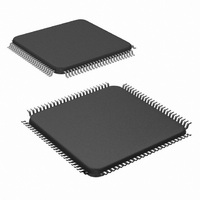
LM9830VJD/NOPB National Semiconductor, LM9830VJD/NOPB Datasheet - Page 39

LM9830VJD/NOPB
Manufacturer Part Number
LM9830VJD/NOPB
Description
IC SCANNER COLOR DOC 100-TQFP
Manufacturer
National Semiconductor
Datasheet
1.LM9830VJDNOPB.pdf
(45 pages)
Specifications of LM9830VJD/NOPB
Number Of Bits
12
Number Of Channels
3
Power (watts)
350mW
Voltage - Supply, Analog
5V
Voltage - Supply, Digital
4.5 V ~ 5.5 V
Package / Case
100-TQFP, 100-VQFP
Lead Free Status / RoHS Status
Lead free / RoHS Compliant
Other names
*LM9830VJD
*LM9830VJD/NOPB
LM9830VJD
*LM9830VJD/NOPB
LM9830VJD
Available stocks
Company
Part Number
Manufacturer
Quantity
Price
Company:
Part Number:
LM9830VJD/NOPB
Manufacturer:
Texas Instruments
Quantity:
10 000
tor for the light source and the stepper motors).
To use the LM9830’s crystal oscillator feature, tie CLK_SEL (pin
71) to DGND
cuit and values for the 48MHz oscillator. The total capacitance on
the CRYSTAL IN node (including PCB capacitance and C1)
should be less than or equal to 10pF.
To drive the LM9830 with an external clock, tie CLK_SEL (pin 71)
to V
CMOS-level clock signal into CRYSTAL_OUT (pin 58).
10.0 Power-On/Reset
When the LM9830 is powered up, a power-on reset signal will
force the RESET and the STANDBY bits high. These bits can
also be controlled through the configuration register.
When the RESET bit is high, the following applies:
The LM9830 enters Transparent mode if using parallel port inter-
face (CMODE = 0).
All state machines are reset. Reset does not affect the values in
the configuration registers (except for those indicated with black
boxes in the Configuration Register table), or the contents of the
gamma RAM or external SRAM.
The STANDBY bit is set by the power on reset signal or by writing
to bit 2 of configuration register 07.
11.0 Standby Mode Conditions
The STANDBY bit is set on power-on.
When the STANDBY bit is high, the following applies:
External I/O (whether in Parallel Port or Microprocessor mode)
continues to function (in order to enter and exit Standby Mode).
All stepper motor outputs are tri-stated.
The 50MHz oscillator continues to run, but MCLK is turned off
inside the LM9830.
Analog blocks are turned off to minimize power consumption.
12.0 Misc. Questions and Answers
Q Where is calibration done?
A Calibration is done on the host computer.
Q Does the LM9830 support 400dpi sensors?
A Yes. Use the 600dpi mode, and understand that the available
horizontal resolutions will be 400, 267, 200, 133, 100, 67, 50,
and 33.
D I/O
CRYSTAL
LM9830
IN (57)
, tie CRYSTAL_IN to DGND
I/O
Figure 63: Crystal Oscillator Circuit
. Figure 63 shows the recommended loading cir-
5pF
C1
Overtone Crystal
EC-T-48.000M
48MHz 3
Ecliptek
15pF
C2
RD
I/O
100
1.2µH
300pF
, and drive the TTL or
CRYSTAL
OUT (58)
LM9830
39
13.0 General Notes and Troubleshooting Tips
If the LM9830 is reset during a scan (Command register > 0), the
gamma table data may be corrupted. Always stop scanning (by
setting Command register to 0) and wait 10 ms before resetting
the LM9830.
Some of the CCD signals (RS, CP1, and CP2) can have a small
pulse when line_end occurs. Line_end resets these signals and
depending on how they are programmed to go on and off,
line_end can chop off the signal before its programmed off time.
If printer power is off, the printer may short the parallel databus to
ground, causing scanner data to be forced to all zeros.
In full duplex modes, the host must read exactly (full - empty)
kbytes from buffer - too few and the LM9830 won’t resume scan-
ning, too many and the LM9830 will output garbage. The full
duplex is mode is not recommended.
The PAUSE bit in the status byte transmitted at the end of a line
represents whether or not a PAUSE REQUEST is currently pend-
ing. This status byte is assembled at the “Line End” point in time
for the line of pixel data just stored in RAM. This signal changes
back to 0 when a RESUME REQUEST is made by the Brain.
(The signal is actually a PAUSE/RESUME REQUEST.)
The PAUSE bit in the status byte at address 02 in the configura-
tion register represents whether or not a PAUSE has actually
occurred.
Registers 4 and 5 only autowrap to 0 from their highest possible
legal address. If an address higher than the highest address is
written, it will continue to increment (not wrap to 0), and unknown
operation may occur. This can not happen unless the host writes
an illegal address to the dataport.
The absolute distance between reference sample and signal
sample must be 2 MCLKs or greater.
The range of values for the Optical Black (registers 0F and 10),
Reset Pulse (11 and 12), CP1 pulse (13 and 14), CP2 pulse (15
and 16), Reference Sample (17), and Signal Sample (18) settings
depend on the rate of the pixel data coming from the sensor.
Register 1 may change state while being read. Always read it
twice in succession to make sure you don’t get erroneous data.
Always make sure line length (data pixels end - data pixels start)
is >= the horizontal divider. For example, if you are dividing by 12,
the line length must be >=12.
The Line End (registers 20 and 21) setting must be programmed
as follows relative to the Data Pixels End (registers 24 and 25)
setting:
Line End must be >= Data Pixels End + 20
The Data Pixels Start (registers 22 and 23) setting must be >=the
Active Pixels Start (registers 1E and 1F) setting.
The MCLK frequency is 25MHz maximum for 12 bit full duplex
mode or 8 bit/8 slot mode.
Data reads in 12 bit half duplex mode can not be done while
scanning.
Pixel Rate Modes
Line Rate Modes
Mode
Pixel Rate
MCLK/24
MCLK/8
http://www.national.com
Registers 0F to 18
Range
0 - 23
0 - 7


