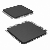
LM9830VJD/NOPB National Semiconductor, LM9830VJD/NOPB Datasheet - Page 2

LM9830VJD/NOPB
Manufacturer Part Number
LM9830VJD/NOPB
Description
IC SCANNER COLOR DOC 100-TQFP
Manufacturer
National Semiconductor
Datasheet
1.LM9830VJDNOPB.pdf
(45 pages)
Specifications of LM9830VJD/NOPB
Number Of Bits
12
Number Of Channels
3
Power (watts)
350mW
Voltage - Supply, Analog
5V
Voltage - Supply, Digital
4.5 V ~ 5.5 V
Package / Case
100-TQFP, 100-VQFP
Lead Free Status / RoHS Status
Lead free / RoHS Compliant
Other names
*LM9830VJD
*LM9830VJD/NOPB
LM9830VJD
*LM9830VJD/NOPB
LM9830VJD
Available stocks
Company
Part Number
Manufacturer
Quantity
Price
Company:
Part Number:
LM9830VJD/NOPB
Manufacturer:
Texas Instruments
Quantity:
10 000
Electrical Characteristics
The following specifications apply for AGND=DGND=DGND
f
CCD/CIS Source Requirements for Full Specified Accuracy and Dynamic Range (Note 12)
Full Channel Characteristics
Coarse Color Balance PGA Characteristics (Configuration Registers 3B, 3C, and 3D)
CRYSTAL IN
V
Absolute Maximum Ratings
Positive Supply Voltage (V
With Respect to
Voltage On Any Input or Output Pin
Input Current at any pin (Note 3)
Package Input Current (Note 3)
Package Dissipation at T
ESD Susceptibility (Note 5)
Soldering Information
Storage Temperature
Symbol
OS PEAK
V
V
V
V
GND=AGND=DGND=DGND
Human Body Model
Infrared, 10 seconds (Note 6)
DNL
INL
OS1
OS1
OS2
OS3
C
= 50MHz. Boldface limits apply for T
Sensor’s Maximum Output Signal
Amplitude before LM9830 Analog Front
End Saturation
Resolution with No Missing Codes
Integral Non-Linearity Error (Note 11)
Differential Non-Linearity
Analog Channel Gain Constant
(ADC Codes/V)
Pre-Boost Analog Channel Offset Error,
CCD Mode
Pre-Boost Analog Channel Offset Error,
CIS Mode
Pre-PGA Analog Channel Offset Error
Post-PGA Analog Channel Offset Error
Monotonicity
G
G
x3 Boost Gain
Gain Error at any gain (Note 13)
0
31
(Minimum PGA Gain)
(Maximum PGA Gain)
A
+
= 25°C
Parameter
=V
A
I/O
=V
=DGND
D
=V
DI/O
SRAM
=V
-0.3V to V
SRAM
-65°C to +150°
(Notes 1 & 2)
A
=T
)
J
=T
(Note 4)
±25mA
±50mA
+
MIN
1000V
235°C
+0.3V
Gain = 0.933
Gain = 3.0
Gain = 9.0
Includes voltage reference
variation, gain setting = 1
PGA Setting = 0
PGA Setting = 31
x3 Boost Setting On
(bit B5 of Gain Register is set)
6.5V
I/O
to T
=DGND
MAX
2
; all other limits T
Operating Ratings
Operating Temperature Range
LM9830VJD
V
V
V
|V
|V
Input Voltage Range
Conditions
A
D
DI/O
A
D
SRAM
-V
Supply Voltage
Supply Voltage
-V
D
SRAM
Supply Voltage
|, |V
=0V, V
A
|, |V
-V
DI/O
A
DI/O
=V
A
|, |V
=T
D
-V
=V
J
SRAM
=25°C. (Notes 7, 8, & 12)
A
DI/O
-V
SRAM
=V
|,
(Note 9)
Typical
SRAM
2048
0.65
0.21
+4.6
+0.7
0.93
3.05
2.99
±0.2
-1.1
-0.5
|, |V
2.1
-30
-21
12
4
(Notes 1 & 2)
=+5.0V
D
-V
DI/O
(Note 10)
-0.05V to V
|,
DC
Limits
http://www.national.com
1863
2129
+2.0
2.98
3.15
2.86
3.08
±1.6
-0.9
,
+10
+34
+38
+14
-21
-15
-58
-59
.90
.96
12
+8
-7
5
+4.5V to +5.5V
+4.5V to +5.5V
+4.5V to +5.5V
0°C T
T
MIN
+
A
LSB (max)
LSB (max)
LSB (max)
LSB (min)
LSB (min)
LSB (min)
V/V (max)
V/V (max)
V/V (max)
mV (max)
mV (max)
mV (max)
mV (max)
T
bits (min)
bits (min)
V/V (min)
V/V (min)
V/V (min)
+ 0.05V
mV (min)
mV (min)
mV (min)
mV (min)
% (max)
(Limits)
100mV
A
+70°C
Units
T
V
V
V
MAX


