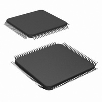
LM9830VJD/NOPB National Semiconductor, LM9830VJD/NOPB Datasheet - Page 23

LM9830VJD/NOPB
Manufacturer Part Number
LM9830VJD/NOPB
Description
IC SCANNER COLOR DOC 100-TQFP
Manufacturer
National Semiconductor
Datasheet
1.LM9830VJDNOPB.pdf
(45 pages)
Specifications of LM9830VJD/NOPB
Number Of Bits
12
Number Of Channels
3
Power (watts)
350mW
Voltage - Supply, Analog
5V
Voltage - Supply, Digital
4.5 V ~ 5.5 V
Package / Case
100-TQFP, 100-VQFP
Lead Free Status / RoHS Status
Lead free / RoHS Compliant
Other names
*LM9830VJD
*LM9830VJD/NOPB
LM9830VJD
*LM9830VJD/NOPB
LM9830VJD
Available stocks
Company
Part Number
Manufacturer
Quantity
Price
Company:
Part Number:
LM9830VJD/NOPB
Manufacturer:
Texas Instruments
Quantity:
10 000
Applications Information
1.0 THEORY OF OPERATION
1.1 Overview
A scanner is composed of many different but tightly intercon-
nected blocks (the analog front end and ADC, sensor clock gen-
eration, stepper motor control, data buffering, parallel port I/O,
and others).
1.2 Signal Processing Overview
1.3 Scanner Support Functions Overview
2.0 Signal Processing Operation
2.1 ADC
The ADC is a 6MHz 12 bit pipelined architecture.
2.2 Pixel Rate Offset Correction Block
Two bytes are used to store the pixel rate offset and gain coeffi-
cients for each pixel. For CCDs, the split is usually 6 bits for offset
and 10 bits for gain. For some CIS sensors with unusually large
offsets, the offset correction range may be increased by changing
the split to 8 bits for offset and 8 bits for gain. This split is deter-
mined by a bit in the configuration register.
A digital subtractor subtracts the 6 (or 8) bit offset word (corre-
sponding to that pixel’s offset error) from each pixel. The LSB of
the offset word is the same size as the 10 bit LSB of the ADC (the
two smallest 12 bit ADC output bits, D1 and D0, are not used with
the offset subtractor). The coefficients are stored in the external
RAM and accessed at the pixel rate.
The subtractor saturates at 0, i.e. if the coefficient to be sub-
tracted is greater than the ADC output code, the result is an out-
put of 0.
2.3 Pixel Rate Gain Correction Block
This is a digital multiplier that multiplies the output word from the
C is a constant that combines the gain error through the AFE, reference voltage variance, and analog voltage
to digital code conversion into one constant. Ideally, C = 2048 codes/V (4096codes/2V). Manufacturing toler-
V
IN
+
V
+
OS1
1V/V or
Boost
3V/V
G
ances widen the range of C. See Electrical Specifications
D
B
OUT
Figure 10: Analog Front End (AFE) Model
= (((V
+
V
+
OS2
simplified, with all offsets = 0, this is:
IN
D
+ V
OUT
+
Offset
DAC
+
OS1
= (V
V
DAC
)G
IN
0.93V/V to
B
23
G
+ V
3V/V
PGA
B
G
subtractor by a 10 (or 8) bit digital correction coefficient corre-
sponding to that pixel’s gain error. The coefficients are stored in
the external RAM and accessed at the pixel rate. When in 8 bit
mode, the 8 bits correspond to the top 8 MSBs of the 10 bit digital
correction coefficient word. The 10 bit LSBs of the input word are
padded with 0s in 8 bit mode.
The multiplier saturates at 1023, i.e. if the result of the multiplica-
tion is greater than 1023, the multiplier output is 1023.
2.4 Pixel Processing Block
2.4.1 Pixel Processing In 8/24 Bit Mode
In the 8 and 10 bit output modes (for 24 and 30 bit color scans),
this stage is where the optical resolution of the sensor is digitally
reduced.
To maximize scanning speed and image quality at the popular
resolutions of 400, 300, 200, 150, 100, 75, and 50 dpi, the resolu-
tion can be reduced inside the scanner, prior to the gamma cor-
rection stage. (Resolution in the vertical direction is controlled by
the stepper motor speed.) This is done by averaging adjacent pix-
els. For example, to get 100 dpi from a 300dpi optical sensor, you
would average 3 300dpi pixels:
The number of pixels out of the Pixel Processing block is equal to
the integer portion of the number of pixels in to the Pixel Process-
ing block divided by the “Divide By” setting, from the table shown
in Figure 11.
If there are not enough pixels at the end of a line to form a com-
plete pixel, the last pixel will be eliminated. For example, if a line
is 35 pixels wide and the Horizontal DPI setting is set to divide by
6, then the output of the Pixel Processing block will be 5 pixels
(the integer portion of 35/6). The last 5 pixels will be discarded,
since 6 pixels would be required to form a new pixel in this mode.
+ V
PGA
DAC
DAC
+ V
+
V
)G
+
OS2
OS3
PGA
)G
C
PGA
pixel
Pixels
+ V
100dpi
12 Bit
ADC
OS1
OUT
)C
=
=
p
------------------------------------------- -
n-2
INT
D
OUT
+
------------------------ -
Divide By
Pixels
p
3
n-1
http://www.national.com
+
IN
p
n


