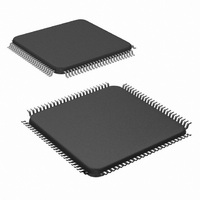
LM9830VJD/NOPB National Semiconductor, LM9830VJD/NOPB Datasheet - Page 33

LM9830VJD/NOPB
Manufacturer Part Number
LM9830VJD/NOPB
Description
IC SCANNER COLOR DOC 100-TQFP
Manufacturer
National Semiconductor
Datasheet
1.LM9830VJDNOPB.pdf
(45 pages)
Specifications of LM9830VJD/NOPB
Number Of Bits
12
Number Of Channels
3
Power (watts)
350mW
Voltage - Supply, Analog
5V
Voltage - Supply, Digital
4.5 V ~ 5.5 V
Package / Case
100-TQFP, 100-VQFP
Lead Free Status / RoHS Status
Lead free / RoHS Compliant
Other names
*LM9830VJD
*LM9830VJD/NOPB
LM9830VJD
*LM9830VJD/NOPB
LM9830VJD
Available stocks
Company
Part Number
Manufacturer
Quantity
Price
Company:
Part Number:
LM9830VJD/NOPB
Manufacturer:
Texas Instruments
Quantity:
10 000
The DataPort allows the user to select a memory block (gamma,
gain coefficient, or offset coefficient) and color (red, green, or
blue) to be read from or written to, by writing to Configuration
Register Address 3.
The starting address of that block (usually 0) is written into the
DataPort Address register (at Configuration Register Addresses 4
and 5). Bit D5 of register 4 should also be set to a 0 or a 1 to indi-
cate whether the DataPort will be read from (D5 = 1) or written to
(D5 = 0) in subsequent operations. This is required so the
LM9830 can prefetch the data for faster access. The DataPort
Address is automatically incremented after every byte of Gamma
data read/written, or every 2 bytes of Offset/Shading data
read/written (since an Offset/Shading word is 2 bytes wide).
Once the memory block, color, and starting address is written, a
series of reads or writes to the DataPort will read from or fill up
that selected memory block at maximum speed.
Registers 4 and 5 should always be (re)written to after register 3
has been changed.
5.1.1 DataPort Type and Color
These 3 bits determine which memory block (gamma or gain/off-
set coefficients, Figure 45) and which color of that memory block
(red, green, or blue, Figure 46) is to be read from or written to.
There is one exception to this: when operating the LM9830 in 1
Channel Mode A, the color is determined by the contents of Reg-
ister 26, bits 3 and 4.
5.1.2 DataPort Address
This 13 bit register (at Configuration Register addresses 4 and 5)
determines what the starting address is for the read/write opera-
tion. This address is automatically incremented after each
read/write operation to the actual DataPort. For the gamma table
the range is 0 to 1023. For the Gain and Offset Coefficients this
range is 0 (corresponding the first valid pixel as programmed in
the Valid Pixels Start register) to 2729 (the maximum number of
7
-
-
7
-
-
-
-
Configuration
6
-
-
6
-
-
-
-
Register
Address
Figure 45: DataPort Target Pointer
Figure 46: DataPort Color Pointer
5
-
-
5
-
-
-
-
5
6
4
-
-
4
-
-
-
-
Figure 44: DataPort
-
-
-
-
-
-
3
3
0
0
1
1
2
-
-
2
DataPort
DataPort
Address
Name
(LSB)
0
1
0
1
1
-
-
1
0
1
0
0
-
-
-
-
Offset & Gain
Undefined
b7 - b0
b7 - b0
Gamma
Bits
Green
Color
Type
Blue
Red
33
image pixels for a 300dpi sensor) or 5460 (the maximum number
of image pixels for a 600dpi sensor). If reads or writes continue
past 1023, 2729, or 5460, the DataPort address counter wraps
back around to 0 and continues counting. Note that for Gain and
Offset Coefficients it takes 2 read/write operations to increment
the address counter, because Gain and Offset Coefficients are
stored as a 2 byte word.
5.1.3 DataPort
This 8 bit register (at Configuration Register address 6) is where
the data is sequentially read from or written to. Gamma data is 8
bits wide. Since offset data may be 6 or 8 bits wide and gain cor-
rection data may be 10 or 8 bits wide, these bytes need to be
combined before they are transmitted. For a 6/10 offset/gain bit
split, the format is shown in Figure 47:
The first byte = Offset * 4 + INT(Gain/256), and
The second byte = Gain AND 255.
An 8/8 offset/gain split is more obvious:
If the offset/gain split is changed from 8/8 to 6/10, or from 6/10 to
8/8, the offset and gain coefficients must be re-calculated and
resent to the LM9830.
In Gamma mode, the DataPort address counter is automatically
incremented after a byte is read from or written to register 6. In
Gain/Offset mode, the DataPort address counter is automatically
incremented after two bytes are read from or written to register 6.
Reading and writing the DataPort should only be done when the
LM9830 is not scanning.
6.0 The Parallel Port Interface
The primary interface of the LM9830 is a PC compatible parallel
port interface. This communication mode is selected by tying the
CMODE pin to DGND. There are two operational parallel port
modes for reading data: Nibble Mode (for compatibility with the
maximum number of existing PCs) and EPP (for maximum speed
on newer machines). In addition, the LM9830 supports a printer
passthrough function that allows an LM9830-based scanner to be
inserted between a PC and a printer.
6.1 The Parallel Port Pins
The parallel port on a standard PC has a total of 17 I/O lines: 8
O5 O4 O3 O2 O1 O0 G9 G8
G7 G6 G5 G4 G3 G2 G1 G0
O7 O6 O5 O4 O3 O2 O1 O0
G7 G6 G5 G4 G3 G2 G1 G0
7
7
Figure 47: DataPort Target Pointer (6/10 split)
Figure 48: DataPort Target Pointer (8/8 split)
6
6
5
5
4
4
3
3
2
2
1
1
0
0
http://www.national.com
Second Byte
Second Byte
First Byte
First Byte
Type
Type


