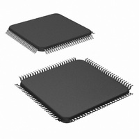
LM9830VJD/NOPB National Semiconductor, LM9830VJD/NOPB Datasheet - Page 30

LM9830VJD/NOPB
Manufacturer Part Number
LM9830VJD/NOPB
Description
IC SCANNER COLOR DOC 100-TQFP
Manufacturer
National Semiconductor
Datasheet
1.LM9830VJDNOPB.pdf
(45 pages)
Specifications of LM9830VJD/NOPB
Number Of Bits
12
Number Of Channels
3
Power (watts)
350mW
Voltage - Supply, Analog
5V
Voltage - Supply, Digital
4.5 V ~ 5.5 V
Package / Case
100-TQFP, 100-VQFP
Lead Free Status / RoHS Status
Lead free / RoHS Compliant
Other names
*LM9830VJD
*LM9830VJD/NOPB
LM9830VJD
*LM9830VJD/NOPB
LM9830VJD
Available stocks
Company
Part Number
Manufacturer
Quantity
Price
Company:
Part Number:
LM9830VJD/NOPB
Manufacturer:
Texas Instruments
Quantity:
10 000
4.3 AFE Operation
The LM9830 supports the following operation modes, controlled
by registers 26 and 27:
• 3 Channel Pixel Rate Mode. In this mode all three channels are
• 3 Channel LIne Rate Mode. In this mode all three channels are
the trailing edge of the first RS pulse. This mode works for TR1
only, under all TR1 settings (normal and CIS TR1 Timing
modes 1 and 2).
converted with the multiplexer in front of the ADC switching at
the ADC conversion rate, producing interleaved RGB data that
is transferred to RAM. The ADC runs at MCLK/8, each chan-
nel’s pixel rate is MCLK/24. Each color has its own offset and
gain coefficients. This mode typically uses Illumination Mode 1.
converted with the multiplexer in front of the ADC switching at
the line rate, producing a line of Red data, followed by a line of
Green data, followed by a line of Blue data, etc. that is trans-
ferred to RAM. The selected channel and the ADC both run at
MCLK/8. Each color has its own offset and gain coefficients.
This mode typically uses Illumination Mode 1.
TR1
RS
C
C
D
C
C
D
ADC Out LIne 1: RGBRGBRGBRGBRGB...
ADC Out LIne 2: RGBRGBRGBRGBRGB...
ADC Out LIne 3: RGBRGBRGBRGBRGB...
ADC Out LIne 4: RGBRGBRGBRGBRGB...
ADC Out LIne 1: RRRRRRRRRRRRRRR...
ADC Out LIne 2: GGGGGGGGGGGGGG...
ADC Out LIne 3: BBBBBBBBBBBBBBBBB...
ADC Out LIne 4: RRRRRRRRRRRRRRR...
Trailing edge of
Figure 36: 3 Channel Pixel Rate Mode
Figure 37: 3 Channel Line Rate Mode
first RS pulse
Figure 35: Fake Optical Black Pixels
Green Channel
Green Channel
Blue Channel
Blue Channel
Red Channel
Red Channel
Pixel-Rate
Multiplexing
Line-Rate
Multiplexing
End of Optical
ADC
ADC
Black Pixels
30
In the 3 Channel Line Rate Mode three TR pulses are generated.
TR
TR
color can be “skipped”, increasing the integration time for that
color. In the example shown in Figure 38, the red channel sees 2
times the integration time of the green channel, and the blue
channel sees 3 times the integration time of the green channel.
Each channel can be independently programmed to drop 0, 1, or
2 TR pulses.
Each color’s TR pulse can be programmed to occur in position 1
(inside Ø1 high) or position 2 (inside Ø1 low), as shown in Figure
39.
• 1 Channel Mode. In this mode only one of the three channels is
There are two variations of 1 Channel Mode:
• 1 Channel Mode A: Uses the selected channel’s offset and gain
TR
TR
TR
Multiplexer
Channel
TR
TR
TR
being converted. That channel and the ADC are clocked at
MCLK/8. The channel is chosen in the configuration register.
coefficients for all lines. This mode typically uses Illumination
Mode 3.
RED
BLUE
Ø1
RED
GREEN
BLUE
RED
GREEN
BLUE
Figure 38: 3 Channel Line Rate TR Pulse Timing
Figure 39: 3 Channel Line Rate Mode with 2 TR
is the TR1 output, TR
is the CP2 output. In this mode TR pulses for a particular
t
INT (RED)
1
Red
2
Pulse Positions
Green
t
INT (GREEN)
GREEN
Blue
1
t
is the TR2 output, and
INT (BLUE)
Red
http://www.national.com
2
Green


