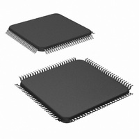
LM9830VJD/NOPB National Semiconductor, LM9830VJD/NOPB Datasheet - Page 3

LM9830VJD/NOPB
Manufacturer Part Number
LM9830VJD/NOPB
Description
IC SCANNER COLOR DOC 100-TQFP
Manufacturer
National Semiconductor
Datasheet
1.LM9830VJDNOPB.pdf
(45 pages)
Specifications of LM9830VJD/NOPB
Number Of Bits
12
Number Of Channels
3
Power (watts)
350mW
Voltage - Supply, Analog
5V
Voltage - Supply, Digital
4.5 V ~ 5.5 V
Package / Case
100-TQFP, 100-VQFP
Lead Free Status / RoHS Status
Lead free / RoHS Compliant
Other names
*LM9830VJD
*LM9830VJD/NOPB
LM9830VJD
*LM9830VJD/NOPB
LM9830VJD
Available stocks
Company
Part Number
Manufacturer
Quantity
Price
Company:
Part Number:
LM9830VJD/NOPB
Manufacturer:
Texas Instruments
Quantity:
10 000
Electrical Characteristics
The following specifications apply for AGND=DGND=DGND
f
DC and Logic Electrical Characteristics
The following specifications apply for AGND=DGND=DGND
f
Static Offset DAC Characteristics (Configuration Registers 38, 39, and 3A)
Analog Input Characteristics
Internal Voltage Reference Characteristics
Digital Input Characteristics for DB0-DB7, D0-D7, STROBE, AUTOFEED, INIT, SELECT IN, PSENSE#1, PSENSE#2, MISC I/O
#1, MISC I/O #2, CMODE
Digital Output Characteristics for DB0-DB7, A0-A17, RD, WR (SRAM Interface)
Digital Output Characteristics for D0-D7, ERROR, ACK, BUSY, PE, SELECT (Parallel Port Interface)
Digital Output Characteristics for MISC I/O #1, MISC I/O #2, A, B, A, B, TR1, TR2, ø1, ø2, RS, CP1, CP2, TRISTATE, LATCH,
LAMP
CRYSTAL IN
CRYSTAL IN
V
Symbol
V
V
Symbol
V
BANDGAP
V
V
V
V
V
V
REF MID
REF LO
V
V
REF HI
OUT(1)
OUT(0)
OUT(1)
OUT(0)
OUT(1)
OUT(0)
C
IN(1)
IN(0)
I
IN
IN
R
, LAMP
= 50MHz. Boldface limits apply for T
= 50MHz. Boldface limits apply for T
Monotonicity
Offset DAC LSB size
Offset DAC Adjustment Range
Average OS
OS
Voltage Reference Output Voltage
Negative Reference Output Voltage
Midpoint Reference Output Voltage
Positive Reference Output Voltage
Logical “1” Input Voltage
Logical “0” Input Voltage
Input Leakage Current
Input Capacitance
Logical “1” Output Voltage
Logical “0” Output Voltage
Logical “1” Output Voltage
Logical “0” Output Voltage
Logical “1” Output Voltage
Logical “0” Output Voltage
G
R
, LAMP
, OS
G
, OS
B
R
, OS
Parameter
B
Parameter
Input Current
G
, OS
B
Input Current
(Continued)
A
A
=T
=T
J
J
=T
=T
MIN
MIN
PGA gain = 1
PGA gain = 1
CDS Enabled, OS = 3.5V
CDS Disabled, OS = 3.5V
V
V
V
V
V
V
V
V
DI/O
DI/O
DI/O
DI/O
DI/O
DI/O
DI/O
DI/O
I/O
I/O
to T
to T
=DGND
=DGND
=5.5V
=4.5V
=4.5V, I
=5.5V, I
=4.5V, I
=5.5V, I
=4.5V, I
=5.5V, I
MAX
MAX
3
; all other limits T
; all other limits T
Conditions
Conditions
SRAM
SRAM
OUT
OUT
OUT
OUT
OUT
OUT
=-4mA
=8mA
=-4mA
=14mA
=-4mA
=8mA
=0V, V
=0V, V
A
A
DC
=V
=V
DC
A
A
=T
=T
D
D
=V
=V
J
J
=25°C. (Notes 7, 8, & 12)
=25°C. (Notes 7 & 8)
DI/O
DI/O
V
=V
V
=V
REF MID
REF MID
(Note 9)
Typical
(Note 9)
SRAM
V
SRAM
Typical
±290
±80
±24
A
±500
9.3
1.2
/2.0
5
+1.0
-1.0
=+5.0V
=+5.0V
(Note 10)
(Note 10)
DC
DC
Limits
Limits
http://www.national.com
±270
12.7
,
±30
,
5.8
2.0
0.8
2.4
0.4
2.4
0.4
2.4
0.4
6
mV (max)
bits (min)
mV (min)
mV (min)
µA (max)
(Limits)
(Limits)
V (max)
V (max)
V (max)
V (max)
V (min)
V (min)
V (min)
V (min)
Units
Units
nA
nA
pF
V
V
V
V


