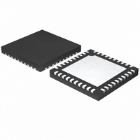
MAX1359BETL+ Maxim Integrated Products, MAX1359BETL+ Datasheet - Page 10

MAX1359BETL+
Manufacturer Part Number
MAX1359BETL+
Description
IC DAS 16BIT 40-TQFN
Manufacturer
Maxim Integrated Products
Type
Data Acquisition System (DAS)r
Specifications of MAX1359BETL+
Resolution (bits)
16 b
Sampling Rate (per Second)
21.84k
Data Interface
Serial
Voltage Supply Source
Analog and Digital
Voltage - Supply
1.8 V ~ 3.6 V
Operating Temperature
-40°C ~ 85°C
Mounting Type
Surface Mount
Package / Case
40-TQFN Exposed Pad
Number Of Converters
2
Resolution
16 bit
Interface Type
Serial (4-Wire, SPI, QSPI, Microwire)
Voltage Reference
1.25 V
Supply Voltage (max)
3.6 V
Supply Voltage (min)
1.8 V
Maximum Power Dissipation
2051.3 mW
Maximum Operating Temperature
+ 85 C
Mounting Style
SMD/SMT
Input Voltage
1.8 V to 3.6 V
Minimum Operating Temperature
- 40 C
Lead Free Status / RoHS Status
Lead free / RoHS Compliant
16-Bit, Data-Acquisition System with ADC, DAC,
UPIOs, RTC, Voltage Monitors, and Temp Sensor
ELECTRICAL CHARACTERISTICS (continued)
(AV
10µF, 10µF between CF+ and CF-, T
10
Note 1:
Note 2:
Note 3:
Note 4:
Note 5:
Note 6:
Note 7:
Note 8:
Note 9:
Note 10: All of the stated temperature accuracies assume that 1) the external diode characteristic is precisely known (i.e., ideal)
Note 11: Values based on simulation results and are not production tested or guaranteed.
Total Supply Current
Sleep-Mode Supply Current
Shutdown Supply Current
DD
______________________________________________________________________________________
= DV
Devices are production tested at T
Guaranteed by design or characterization.
The offset and gain errors are corrected by self-calibration. The calibration process requires measurement to be made at
the selected data rate. The calibration error is therefore in the order of peak-to-peak noise for the selected rate.
Eliminate drift errors by recalibration at the new temperature.
The gain error excludes reference error, offset error (unipolar), and zero error (bipolar).
Gain-error drift does not include unipolar offset drift or bipolar zero-error drift. It is effectively the drift of the part if zero-
scale error is removed.
These specs are obtained from characterization during design or from initial product evaluation. Not production tested or
guaranteed.
OUTA/B = +0.5V or +1.5V, SWA/B = +1.5V or +0.5V, T
Long-term stability is characterized using five to six parts. The bandgaps are turned on for 1000hrs at room temperature
with the parts running continuously. Daily measurements are taken and any obvious outlying data points are discarded.
and 2) the ADC reference voltage is exactly equal to 1.25V. Any variations to this known reference characteristic and volt-
age caused by temperature, loading, or power supply results in errors in the temperature measurement. The actual tem-
perature calculation is performed externally by the microcontroller (µC).
PARAMETER
DD
= +1.8V to +3.6V, V
A
REF
= T
SYMBOL
I
NORMAL
I
I
SLEEP
= +1.25V, external reference, f
SHDN
I
MIN
MAX
to T
A
= +25°C and T
MAX
Everything on,
charge pump
unloaded, max
internal temp-sensor
current, clock output
buffers unloaded,
ADC at 512sps
All on except charge pump and temp
sensor, ADC at 512sps, CLK output buffer
enabled, clock output buffers unloaded
T
T
All off
A
A
, unless otherwise noted. Typical values are at T
= -45°C to +85°C
= +25°C
A
= +85°C. Specifications to T
CONDITIONS
A
= 0°C to +50°C.
CLK32K
AV
AV
AV
AV
AV
AV
T
T
A
A
DD
DD
DD
DD
DD
DD
= -40°C to +85°C
= +25°C
= 32.768kHz (external clock), C
= DV
= DV
= DV
= DV
= DV
= DV
DD
DD
DD
DD
DD
DD
= 3.6V
= 3.3V
= 3.0V
= 3.6V
= 3.0V
= 3.6V
A
= -40°C are guaranteed by design.
MIN
A
= +25°C.) (Note 1)
TYP
1.36
1.15
1.17
5.18
6.15
4.42
5.56
1.6
REG
= 10µF, C
MAX
5.19
2.0
1.7
1.3
6.5
8.3
9
4
CPOUT
UNITS
mA
µA
µA
=


