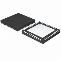
MAX1359BETL+ Maxim Integrated Products, MAX1359BETL+ Datasheet - Page 59

MAX1359BETL+
Manufacturer Part Number
MAX1359BETL+
Description
IC DAS 16BIT 40-TQFN
Manufacturer
Maxim Integrated Products
Type
Data Acquisition System (DAS)r
Specifications of MAX1359BETL+
Resolution (bits)
16 b
Sampling Rate (per Second)
21.84k
Data Interface
Serial
Voltage Supply Source
Analog and Digital
Voltage - Supply
1.8 V ~ 3.6 V
Operating Temperature
-40°C ~ 85°C
Mounting Type
Surface Mount
Package / Case
40-TQFN Exposed Pad
Number Of Converters
2
Resolution
16 bit
Interface Type
Serial (4-Wire, SPI, QSPI, Microwire)
Voltage Reference
1.25 V
Supply Voltage (max)
3.6 V
Supply Voltage (min)
1.8 V
Maximum Power Dissipation
2051.3 mW
Maximum Operating Temperature
+ 85 C
Mounting Style
SMD/SMT
Input Voltage
1.8 V to 3.6 V
Minimum Operating Temperature
- 40 C
Lead Free Status / RoHS Status
Lead free / RoHS Compliant
For a unipolar output, the output voltages and the refer-
ence have the same polarity. Figure 22 shows the
MAX1359B’s unipolar output circuit, which is also the
typical operating circuit for the DAC. Table 22 lists
some unipolar input codes and their corresponding
output voltages.
For larger output swing, see Figure 23. This circuit
shows the output amplifiers configured with a closed-
loop gain of +2V/V to provide 0 to 2.5V full-scale range
with the 1.25V reference.
The MAX1359B DAC outputs can be configured for bipo-
lar operation using the application circuit in Figure 24:
where N is the decimal value of the DAC’s binary input
code.
Figure 21. ADC Bipolar Transfer Function
Table 22. Unipolar Code
UPIOs, RTC, Voltage Monitors, and Temp Sensor
16-Bit, Data-Acquisition System with ADC, DAC,
0111 1111 1111 1111
0111 1111 1111 1110
0111 1111 1111 1101
0000 0000 0000 0001
0000 0000 0000 0000
1111 1111 1111 1111
1000 0000 0000 0010
1000 0000 0000 0001
1000 0000 0000 0000
DAC CONTENTS
MSB
1111 1111 11
1000 0000 01
1000 0000 00
0111 1111 11
0000 0000 01
0000 0000 00
-32,768
V
OUT
LSB
1 LSB =
______________________________________________________________________________________
-32,766
=
V
(GAIN x 65,536)
REF
/GAIN
V
V
REF
REF
INPUT VOLTAGE (LSB)
⎡
⎢
⎣
+V
DAC Unipolar Output
-1
x 2
⎛
⎜
⎝
DAC Bipolar Output
1024
REF
0
2
N
ANALOG OUTPUT
+V
+V
+V
+1
(512/1024) = +V
+V
⎞
⎟ −
⎠
REF
REF
REF
REF
V
1
(1023/1024)
REF
(513/1024)
(511/1024)
⎤
⎥
⎦
+32,765
(1/1024)
0
/GAIN
+32,767
REF
/ 2
Table 23 shows digital codes (offset binary) and corre-
sponding output voltages for Figure 24 assuming
R1 = R2.
Figure 22. DAC Unipolar Output Circuit
Figure 23. DAC Unipolar Rail-to-Rail Output Circuit
Table 23. Bipolar Code
V
REF
REF
DAC CONTENTS
= 1.25V
REF
1111 1111 11
1000 0000 01
1000 0000 00
0111 1111 11
0000 0000 01
0000 0000 00
MSB
MAX1359B
MAX1359B
DAC A
LSB
DAC A
-V
REF
ANALOG OUTPUT
+V
-V
FBA
+V
-V
REF
(512/512) = -V
REF
REF
FBA
REF
(511/512)
10kΩ
(511/512)
0
(1/512)
(1/512)
10kΩ
OUTA
OUTA
REF
59


