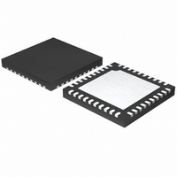
MAX1359BETL+ Maxim Integrated Products, MAX1359BETL+ Datasheet - Page 29

MAX1359BETL+
Manufacturer Part Number
MAX1359BETL+
Description
IC DAS 16BIT 40-TQFN
Manufacturer
Maxim Integrated Products
Type
Data Acquisition System (DAS)r
Specifications of MAX1359BETL+
Resolution (bits)
16 b
Sampling Rate (per Second)
21.84k
Data Interface
Serial
Voltage Supply Source
Analog and Digital
Voltage - Supply
1.8 V ~ 3.6 V
Operating Temperature
-40°C ~ 85°C
Mounting Type
Surface Mount
Package / Case
40-TQFN Exposed Pad
Number Of Converters
2
Resolution
16 bit
Interface Type
Serial (4-Wire, SPI, QSPI, Microwire)
Voltage Reference
1.25 V
Supply Voltage (max)
3.6 V
Supply Voltage (min)
1.8 V
Maximum Power Dissipation
2051.3 mW
Maximum Operating Temperature
+ 85 C
Mounting Style
SMD/SMT
Input Voltage
1.8 V to 3.6 V
Minimum Operating Temperature
- 40 C
Lead Free Status / RoHS Status
Lead free / RoHS Compliant
An internal oscillator and a frequency-locked loop (FLL)
are used to generate a 4.9152MHz ±1% high-frequen-
cy clock. This clock and derivatives are used internally
by the ADC, analog switches, and PWM. This clock sig-
nal outputs to CLK. When the FLL is enabled, the high-
frequency clock is locked to the 32.768kHz reference.
If the FLL is disabled, the high-frequency clock is free-
running. At power-up, the CLK pin defaults to a
2.4576MHz clock output, which is compatible with most
µCs. See Figure 12 for a block diagram of the high-fre-
quency clock.
The MAX1359B provides four digital programmable
I/Os (UPIO1–UPIO4). Configure UPIOs as logic inputs
or outputs using the UPIO control register. Configure
the internal pullups using the UPIO setup register, if
Figure 11. Watchdog Timer Block Diagram
Figure 12. High-Frequency Clock and FLL Block Diagram
UPIOs, RTC, Voltage Monitors, and Temp Sensor
16-Bit, Data-Acquisition System with ADC, DAC,
M32K
32K
______________________________________________________________________________________
POR PULSES HIGH DURING POWER-UP.
WDW PULSES HIGH DURING WATCHDOG REGISTER WRITE.
FLLE
WDE
FREQUENCY
COMPARE
User-Programmable I/Os
High-Frequency Clock
ERROR
FREQ
BY-8192
DIVIDE-
WDW
POR
32.768kHz
INTEGRATOR
FREQUENCY
4Hz
TUNE<8:0>
D
CK
R
Q
Q
CONTROLLED
OSCILLATOR
DIGITALLY
HFCE
required. At power-up, the UPIO’s are internally pulled
up to DV
or CPOUT. See the UPIO__CTRL Register and
UPIO_SPI Register sections for more details on config-
uring the UPIO_ pins.
Program each UPIO1–UPIO4 as one of the following:
• General-purpose input
• Power-mode control
• Analog switch (SPST) and SPDT control input
• ADC data-ready output
• General-purpose output
• PWM output
• Alarm output
• SPI passthrough
DD
CKSEL2
0
1
MUX
2:1
. UPIO_ outputs can be referenced to DV
CK
D
4.9152MHz HF OSCILLATOR AND FLL
R
Q
Q
CKSEL<1:0>
4.9152MHz
1, 2, 4, 8
DIVIDER
WATCHDOG TIMER
CLKE
WDTO
CRDY
HFCLK
CLK
DD
29


