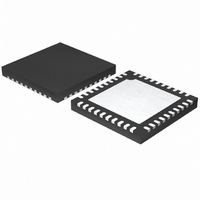
MAX1359BETL+ Maxim Integrated Products, MAX1359BETL+ Datasheet - Page 51

MAX1359BETL+
Manufacturer Part Number
MAX1359BETL+
Description
IC DAS 16BIT 40-TQFN
Manufacturer
Maxim Integrated Products
Type
Data Acquisition System (DAS)r
Specifications of MAX1359BETL+
Resolution (bits)
16 b
Sampling Rate (per Second)
21.84k
Data Interface
Serial
Voltage Supply Source
Analog and Digital
Voltage - Supply
1.8 V ~ 3.6 V
Operating Temperature
-40°C ~ 85°C
Mounting Type
Surface Mount
Package / Case
40-TQFN Exposed Pad
Number Of Converters
2
Resolution
16 bit
Interface Type
Serial (4-Wire, SPI, QSPI, Microwire)
Voltage Reference
1.25 V
Supply Voltage (max)
3.6 V
Supply Voltage (min)
1.8 V
Maximum Power Dissipation
2051.3 mW
Maximum Operating Temperature
+ 85 C
Mounting Style
SMD/SMT
Input Voltage
1.8 V to 3.6 V
Minimum Operating Temperature
- 40 C
Lead Free Status / RoHS Status
Lead free / RoHS Compliant
UPIO SPI pass-through control register. These bits map
the serial interface signals to the UPIO pins, allowing the
DAS (MAX1359B) to drive other devices at CPOUT or
DV
found in the UPIO_CTRL register. Individual bits are pro-
vided to set only the desired UPIO inputs to the SPI
pass-through mode. This mode becomes active when
CS is driven high to complete the write to this register,
and remains active as long as CS stays high (i.e., multi-
ple pass-through writes are possible). The SPI pass-
through mode is deactivated immediately when CS is
pulled low for the next DAS (MAX1359B) write.
The UPIO_ state (both before and after the SPI pass-
through mode) is set by the UP_MD<3:0> and LL_ bits.
When a UPIO is configured for SPI pass-through mode
and the CS is high, UPR_, UPF_, and LL_ continue to
detect UPIO_ edges, which can still generate interrupts.
See Figure 18 for an SPI pass-through timing diagram.
UPIO_SPI Register (Power-On State: 0000 XXXX)
Figure 18. SPI Pass-Through Timing Diagram
UPIOs, RTC, Voltage Monitors, and Temp Sensor
16-Bit, Data-Acquisition System with ADC, DAC,
DD
UPIO4
UPIO3
UPIO2
UPIO1
DOUT
SCLK
UP4S
DIN
MSB
CS
voltage levels, depending on the SV_ bit setting
D
N
D
WRITE TO DAS TO ENABLE SPI MODE
N-1
SET BY UPIO4_CTRL REGISTER
SET BY UPIO3_CTRL REGISTER
SET BY UPIO2_CTRL REGISTER
SET BY UPIO1_CTRL REGISTER
______________________________________________________________________________________
D
UP3S
N-2
D
N-3
D
3
D
2
UP2S
D
1
D
0
E
E
N
N
UP1S
E
E
WRITE THROUGH DAS TO UPIO DEVICE
N-1
N-1
E
E
N-2
N-2
E
E
N-3
N-3
UP4S: UPIO4 SPI pass-through-mode enable bit. A
logic 1 maps the inverted CS signal to the UPIO4 pin.
Therefore, UPIO4 is low (near DGND) when SPI pass-
through mode is active, and is high (near DV
CPOUT) when the mode is inactive. A logic 0 disables
the UPIO4 SPI pass-through mode. The power-on
default is 0.
UP3S: UPIO3 SPI pass-through-mode enable bit. A
logic 1 maps the SCLK signal to UPIO3 (directly with no
inversion), while a logic 0 disables the UPIO3 SPI pass-
through mode. The power-on default is 0.
UP2S: UPIO2 SPI pass-through-mode enable bit. A
logic 1 maps the DIN signal to UPIO2 (directly with no
inversion), while a logic 0 disables the UPIO2 SPI pass-
through mode. The power-on default is 0.
UP1S: UPIO1 SPI pass-through-mode enable bit. A
logic 1 maps the UPIO1 input signal to DOUT (directly
with no inversion), while a logic 0 disables the UPIO1
SPI pass-through mode. The power-on default is 0.
E
E
X
X
3
3
X
E
E
X
X
2
2
E
E
X
X
1
1
E
E
X
X
0
0
D
X
7
D
6
SET BY UPIO4_CTRL REGISTER
SET BY UPIO3_CTRL REGISTER
SET BY UPIO2_CTRL REGISTER
SET BY UPIO1_CTRL REGISTER
NORMAL WRITE TO DAS
D
5
D
4
X
D
3
D
2
D
1
LSB
D
X
0
DD
51
or


