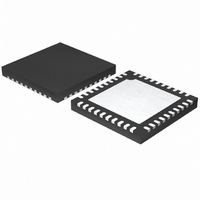
MAX1359BETL+ Maxim Integrated Products, MAX1359BETL+ Datasheet - Page 37

MAX1359BETL+
Manufacturer Part Number
MAX1359BETL+
Description
IC DAS 16BIT 40-TQFN
Manufacturer
Maxim Integrated Products
Type
Data Acquisition System (DAS)r
Specifications of MAX1359BETL+
Resolution (bits)
16 b
Sampling Rate (per Second)
21.84k
Data Interface
Serial
Voltage Supply Source
Analog and Digital
Voltage - Supply
1.8 V ~ 3.6 V
Operating Temperature
-40°C ~ 85°C
Mounting Type
Surface Mount
Package / Case
40-TQFN Exposed Pad
Number Of Converters
2
Resolution
16 bit
Interface Type
Serial (4-Wire, SPI, QSPI, Microwire)
Voltage Reference
1.25 V
Supply Voltage (max)
3.6 V
Supply Voltage (min)
1.8 V
Maximum Power Dissipation
2051.3 mW
Maximum Operating Temperature
+ 85 C
Mounting Style
SMD/SMT
Input Voltage
1.8 V to 3.6 V
Minimum Operating Temperature
- 40 C
Lead Free Status / RoHS Status
Lead free / RoHS Compliant
The OFFSET CAL register contains the 24-bit data of
the most recently completed offset calibration.
is two’s complement and is subtracted from the ADC
output before being written to the DATA register. The
offset calibration allows input offset errors between
V
The MAX1359B can perform system offset calibration
Table 9. Selecting the Negative MUX Inputs
X = Don’t care.
DATA Register (Power-On State: 0000 0000 0000 0000)
ADC<15:0> Analog-to-digital conversion data bits. These 16 bits are the results from the most recently completed
conversion. The data format is unsigned, binary for unipolar mode, and two’s complement for bipolar mode.
OFFSET CAL Register (Power-On State: 0000 0000 0000 0000 0000
OFFSET<23:0>: Offset-calibration bits. The data format
REF
UPIOs, RTC, Voltage Monitors, and Temp Sensor
OFFSET23
OFFSET15
16-Bit, Data-Acquisition System with ADC, DAC,
OFFSET7
ADC15
NEGATIVE MUX INPUT
ADC7
MSB
MSB
±50% to be corrected in unipolar or bipolar mode.
TEMP-
AGND
SNO2
OUTA
SCM2
OUT2
SNC2
OUT1
Open
AIN2
REF
OFFSET22
OFFSET14
OFFSET6
______________________________________________________________________________________
ADC14
ADC6
OFFSET21
OFFSET13
OFFSET5
ADC13
ADC5
MUXN3
0
0
0
0
0
0
0
0
1
1
1
1
OFFSET20
OFFSET12
OFFSET4
ADC12
ADC4
MUXN2
or self offset calibration. Self-calibration performs a cali-
bration for the entire signal path. See the ADC
Calibration section for more details.
The ADC input voltage range specifications must
always be obeyed and the OFFSET CAL register effec-
tively offsets the ADC digital scale to a “zero” value
determined by the calibration.
OFFSET19
OFFSET11
OFFSET3
0
0
0
0
1
1
1
1
0
0
0
1
ADC11
ADC3
0000)
OFFSET18
OFFSET10
OFFSET2
ADC10
ADC2
MUXN0
X
0
0
1
1
0
0
1
1
0
0
1
OFFSET17
OFFSET9
OFFSET1
ADC9
ADC1
LSB
MUXN0
OFFSET16
X
X
0
1
0
1
0
1
0
1
0
1
OFFSET8
OFFSET0
ADC8
ADC0
LSB
37


