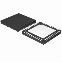
MAX1359BETL+ Maxim Integrated Products, MAX1359BETL+ Datasheet - Page 52

MAX1359BETL+
Manufacturer Part Number
MAX1359BETL+
Description
IC DAS 16BIT 40-TQFN
Manufacturer
Maxim Integrated Products
Type
Data Acquisition System (DAS)r
Specifications of MAX1359BETL+
Resolution (bits)
16 b
Sampling Rate (per Second)
21.84k
Data Interface
Serial
Voltage Supply Source
Analog and Digital
Voltage - Supply
1.8 V ~ 3.6 V
Operating Temperature
-40°C ~ 85°C
Mounting Type
Surface Mount
Package / Case
40-TQFN Exposed Pad
Number Of Converters
2
Resolution
16 bit
Interface Type
Serial (4-Wire, SPI, QSPI, Microwire)
Voltage Reference
1.25 V
Supply Voltage (max)
3.6 V
Supply Voltage (min)
1.8 V
Maximum Power Dissipation
2051.3 mW
Maximum Operating Temperature
+ 85 C
Mounting Style
SMD/SMT
Input Voltage
1.8 V to 3.6 V
Minimum Operating Temperature
- 40 C
Lead Free Status / RoHS Status
Lead free / RoHS Compliant
16-Bit, Data-Acquisition System with ADC, DAC,
UPIOs, RTC, Voltage Monitors, and Temp Sensor
The switch-control register controls the two SPDT
switches (SPDT1 and SPDT2) and the DACA output
buffer SPST switch (SWA). Control these switches by
the serial bits in this register, by any of the UPIO pins
that are enabled for that function, or by the PWM.
SWA: (MAX1359B) DACA output buffer SPST-switch A
control bit. The SWA bit, the UPIO inputs (if configured),
and the PWM (if configured) control the state of the
SWA switch as shown in Table 17. The UPIO_ states of
0 and 1 in Table 17 correspond to respective deassert-
ed and asserted logic states as defined by the ALH_ bit
of the UPIO_CTRL register. If a UPIO is not configured
for this mode, its value applied to Table 17 is 0. The
PWM states of 0 and 1 in the table below correspond to
the respective PWM off (or low) and on (or high) states
defined by the SWAH and SWAL bits (see the
PWM_CTRL Register section). If the PWM is not config-
SW_CTRL Register (Power-On State: 0000 00XX)
Table 17. SWA States
X = Don’t care.
* Switch SWA control is effectively an OR of the SWA bit, UPIO
pins, and PWM.
52
SWA BIT*
______________________________________________________________________________________
0
X
X
1
MSB
SWA
UPIO_*
0
X
1
X
0
PWM*
0
1
X
X
SPDT11
SWA SWITCH STATE
Switch open
Switch closed
Switch closed
Switch closed
SPDT10
ured for this mode, its value applied to the table below
is 0. The power-on default is 0.
SPDT1<1:0>: Single-pole double-throw switch 1 con-
trol bits. The SPDT1<1:0> bits, the UPIO pins (if config-
ured), and the PWM (if configured) control the state of
the switch as shown in Table 18. The UPIO_ states of 0
and 1 in Table18 correspond to respective deasserted
and asserted logic states as defined by the ALH_ bit of
the UPIO_CTRL register. If a UPIO is not configured for
this mode, its value applied to Table 18 is 0. The PWM
states of 0 and 1 in Table 18 below correspond to the
respective PWM off (low) and on (high) states defined
by the SPD1 bit in the PWM_CTRL register. If the PWM
is not configured for this mode, its value applied to
Table 18 is 0. The power-on default is 00.
Table 18. SPDT Switch 1 States
X = Don’t care.
* Switch SPDT1 control is effectively an OR of the SPDT10 bit, the
UPIO pins, and the PWM output. The SPDT11 bit determines if
the switches open and close together or if they toggle.
SPDT1<1:0>
SPDT21
0
0
0
0
1
1
1
1
0
X
X
1
0
X
X
1
UPIO_* PWM* SPDT1 SWITCH STATE
SPDT20
X
X
X
X
0
1
0
1
0
1
X
X
0
1
X
X
SNO1 open, SNC1 open
SNO1 closed, SNC1 closed
SNO1 closed, SNC1 closed
SNO1 closed, SNC1 closed
SNC1 closed, SNO1 open
SNC1 open, SNO1 closed
SNC1 open, SNO1 closed
SNC1 open, SNO1 closed
X
LSB
X


