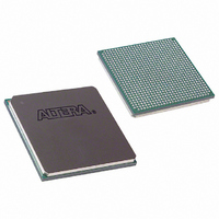
EP3C120F780I7 Altera, EP3C120F780I7 Datasheet - Page 14

EP3C120F780I7
Manufacturer Part Number
EP3C120F780I7
Description
IC CYCLONE III FPGA 120K 780FBGA
Manufacturer
Altera
Series
Cyclone® IIIr
Datasheets
1.EP3C5F256C8N.pdf
(5 pages)
2.EP3C5F256C8N.pdf
(34 pages)
3.EP3C5F256C8N.pdf
(66 pages)
4.EP3C5F256C8N.pdf
(14 pages)
5.EP3C5F256C8N.pdf
(76 pages)
6.EP3C120F780I7.pdf
(274 pages)
Specifications of EP3C120F780I7
Number Of Logic Elements/cells
119088
Number Of Labs/clbs
7443
Total Ram Bits
3981312
Number Of I /o
531
Voltage - Supply
1.15 V ~ 1.25 V
Mounting Type
Surface Mount
Operating Temperature
-40°C ~ 100°C
Package / Case
780-FBGA
Family Name
Cyclone III
Number Of Logic Blocks/elements
119088
# I/os (max)
531
Frequency (max)
437.5MHz
Process Technology
65nm
Operating Supply Voltage (typ)
1.2V
Logic Cells
119088
Ram Bits
3981312
Operating Supply Voltage (min)
1.15V
Operating Supply Voltage (max)
1.25V
Operating Temp Range
-40C to 100C
Operating Temperature Classification
Industrial
Mounting
Surface Mount
Pin Count
780
Package Type
FBGA
For Use With
544-2589 - KIT DEV EMB CYCLONE III EDITION544-2566 - KIT DEV DSP CYCLONE III EDITION544-2444 - KIT DEV CYCLONE III EP3C120
Lead Free Status / RoHS Status
Contains lead / RoHS non-compliant
Number Of Gates
-
Lead Free Status / Rohs Status
Not Compliant
Available stocks
Company
Part Number
Manufacturer
Quantity
Price
Part Number:
EP3C120F780I7
Manufacturer:
ALTERA/阿尔特拉
Quantity:
20 000
Company:
Part Number:
EP3C120F780I7N
Manufacturer:
ALTERA
Quantity:
118
Page 14
Table 6. Compensation Modes
areset
locked
pfdena
Signal
f
1
Table 5. Compensation Modes
PLL Dynamic Reconfiguration and Phase Stepping
You can use this feature if you want to change the PLL settings without needing to
reconfigure the entire device. Two main applications for this feature change between
two output frequencies to suit the design and to adjust the clock-to-output (t
in real time without the need to regenerate a configuration file with new PLL settings.
You can enable the dynamic reconfiguration feature by instantiating the altpll
megafunction. Then, you can ease the usage of this feature by instantiating the
altpll_reconfig megafunction.
To obtain the maximum reconfiguration clock frequency (fscanclk) and typical time
required to reconfigure the scan chains (tconfigpll), refer to the
Datasheet: DC and Switching Characteristics
Handbook.
PLL Control Signals
There are three main control signals, which are essential during PLL usage,
depending on the application.
Source-synchronous
Mode
No Compensation
Mode
Normal Mode
Zero Delay Buffer
(ZDB) Mode
When enabled, this control pin is an input reset pin for each PLL. You must enable this control pin
if you enable the dynamic reconfiguration and clock switchover feature. You should also enable the
automatic reset upon loss of lock feature using the altpll megafunction so that the PLL resets
automatically when the locked signal goes low.
Refer to the
the Cyclone III Device Handbook to obtain the minimum pulse width on the
When enabled, this control pin is an output pin for each PLL. When it is high, the PLL has locked
onto the reference clock and the PLL clock outputs are operating at the desired phase and
frequency. You should create a design to monitor this signal to ensure that the system using the
PLL clock outputs reacts according to the validity of clock output.
When enabled, this control pin is an input pin for each PLL. You should enable this pin if your
system requires a certain clock frequency from the PLL even though the input clock is disabled, so
that it will have time to store its current setting before shutting down.
Modes
Cyclone III Device Datasheet: DC and Switching Characteristics
Choose this mode if you want to maintain the same phase relationship
between the clock and data from the input pins to the I/O element (IOE)
register driven by the PLL.
Choose this mode if you want a better jitter performance at the PLL
output.
Choose this mode if you want the clock edge at an IOE or Logic Element
(LE) register driven by the PLL to be phase-aligned with the clock signal at
the clock input pin.
Choose this mode if you want the external clock output pin to be
phase-aligned with the clock input pin for zero delay through the device.
Description
chapter in volume 2 of the Cyclone III Device
Description
© November 2008 Altera Corporation
areset
chapter in volume 2 of
Cyclone III Device
Early System Planning
signal (t
CO
) delays
ARESET
).


