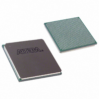
EP3C120F780I7 Altera, EP3C120F780I7 Datasheet - Page 41

EP3C120F780I7
Manufacturer Part Number
EP3C120F780I7
Description
IC CYCLONE III FPGA 120K 780FBGA
Manufacturer
Altera
Series
Cyclone® IIIr
Datasheets
1.EP3C5F256C8N.pdf
(5 pages)
2.EP3C5F256C8N.pdf
(34 pages)
3.EP3C5F256C8N.pdf
(66 pages)
4.EP3C5F256C8N.pdf
(14 pages)
5.EP3C5F256C8N.pdf
(76 pages)
6.EP3C120F780I7.pdf
(274 pages)
Specifications of EP3C120F780I7
Number Of Logic Elements/cells
119088
Number Of Labs/clbs
7443
Total Ram Bits
3981312
Number Of I /o
531
Voltage - Supply
1.15 V ~ 1.25 V
Mounting Type
Surface Mount
Operating Temperature
-40°C ~ 100°C
Package / Case
780-FBGA
Family Name
Cyclone III
Number Of Logic Blocks/elements
119088
# I/os (max)
531
Frequency (max)
437.5MHz
Process Technology
65nm
Operating Supply Voltage (typ)
1.2V
Logic Cells
119088
Ram Bits
3981312
Operating Supply Voltage (min)
1.15V
Operating Supply Voltage (max)
1.25V
Operating Temp Range
-40C to 100C
Operating Temperature Classification
Industrial
Mounting
Surface Mount
Pin Count
780
Package Type
FBGA
For Use With
544-2589 - KIT DEV EMB CYCLONE III EDITION544-2566 - KIT DEV DSP CYCLONE III EDITION544-2444 - KIT DEV CYCLONE III EP3C120
Lead Free Status / RoHS Status
Contains lead / RoHS non-compliant
Number Of Gates
-
Lead Free Status / Rohs Status
Not Compliant
Available stocks
Company
Part Number
Manufacturer
Quantity
Price
Part Number:
EP3C120F780I7
Manufacturer:
ALTERA/阿尔特拉
Quantity:
20 000
Company:
Part Number:
EP3C120F780I7N
Manufacturer:
ALTERA
Quantity:
118
Design and Compilation
PLL Considerations
© November 2008 Altera Corporation
f
f
f
For more information on the support and implementation, refer to the On-Chip
Termination Support section in the
the Cyclone III Device Handbook.
Dedicated Differential Output Buffer with Programmable Pre-Emphasis
Cyclone III devices provide dedicated differential output buffers on left and right I/O
banks. These buffers are capable of transmitting LVDS signals at up to 840 Mbps
without requiring external resistors. Similarly, you can transmit RSDS, mini-LVDS,
and PPDS with dedicated transmitter buffers with no external resistors required at
different speeds. Only a differential termination resistor is required on the receiver.
The top and bottom I/O banks can transmit differential I/O standards, but require an
additional resistor network on the transmitter. You can implement the serializer and
deserializer (SERDES) for LVDS using the altlvds megafunction in the Quartus II
software. SERDES is implemented in core logic as Cyclone III devices do not have a
dedicated SERDES circuit.
For more information on the support and implementation, refer to the
Differential Interfaces in Cyclone III Devices
Handbook.
Programmable pre-emphasis is supported on dedicated differential output buffers to
maximize the data eye opening at the far-end receiver. High speed interfaces that use
long traces typically suffer high frequency signal attenuation in the transmission
media due to skin effect and dielectric loss. Programmable pre-emphasis reduces the
attenuation, by boosting high frequency component at each transition in the data
stream. To enable this in the Quartus II software, set Programmable Pre-emphasis
assignment for the pin to On in the Assignment Editor.
Post PLL Design
After designing the PLL, consider the following topics before designing the board.
Choosing the PLL
For Cyclone III devices, there are four identical PLLs (except EP3C5 and EP3C10,
which have only two identical PLLs). You can choose to use a specific PLL or let the
Quartus II software choose the best PLL to use. For the first option, you must choose
the PLL where you have available suitable dedicated input and output clock pins. The
PLL input clock must be either dedicated input clock pins or another PLL output. The
PLL input clock cannot be driven from internal logic. The PLL output clock should be
connected to its dedicated clock output pin for optimum routing (only applies to c0),
user I/O, or global clock (GCLK).
To obtain the locations of the PLLs and their corresponding pins, refer to the
corresponding device pin-outs and
chapter in volume 1 of the Cyclone III Device Handbook.
Pin Assignment
The following are the recommended pin assignments in the Quartus II software for
the PLL input and output ports.
Cyclone III Device I/O Features
Clock Networks and PLLs in Cyclone III Devices
chapter in volume 1 of the Cyclone III Device
chapter in volume 1 of
High-Speed
Page 41


