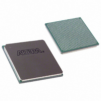
EP3C120F780I7 Altera, EP3C120F780I7 Datasheet - Page 5

EP3C120F780I7
Manufacturer Part Number
EP3C120F780I7
Description
IC CYCLONE III FPGA 120K 780FBGA
Manufacturer
Altera
Series
Cyclone® IIIr
Datasheets
1.EP3C5F256C8N.pdf
(5 pages)
2.EP3C5F256C8N.pdf
(34 pages)
3.EP3C5F256C8N.pdf
(66 pages)
4.EP3C5F256C8N.pdf
(14 pages)
5.EP3C5F256C8N.pdf
(76 pages)
6.EP3C120F780I7.pdf
(274 pages)
Specifications of EP3C120F780I7
Number Of Logic Elements/cells
119088
Number Of Labs/clbs
7443
Total Ram Bits
3981312
Number Of I /o
531
Voltage - Supply
1.15 V ~ 1.25 V
Mounting Type
Surface Mount
Operating Temperature
-40°C ~ 100°C
Package / Case
780-FBGA
Family Name
Cyclone III
Number Of Logic Blocks/elements
119088
# I/os (max)
531
Frequency (max)
437.5MHz
Process Technology
65nm
Operating Supply Voltage (typ)
1.2V
Logic Cells
119088
Ram Bits
3981312
Operating Supply Voltage (min)
1.15V
Operating Supply Voltage (max)
1.25V
Operating Temp Range
-40C to 100C
Operating Temperature Classification
Industrial
Mounting
Surface Mount
Pin Count
780
Package Type
FBGA
For Use With
544-2589 - KIT DEV EMB CYCLONE III EDITION544-2566 - KIT DEV DSP CYCLONE III EDITION544-2444 - KIT DEV CYCLONE III EP3C120
Lead Free Status / RoHS Status
Contains lead / RoHS non-compliant
Number Of Gates
-
Lead Free Status / Rohs Status
Not Compliant
Available stocks
Company
Part Number
Manufacturer
Quantity
Price
Part Number:
EP3C120F780I7
Manufacturer:
ALTERA/阿尔特拉
Quantity:
20 000
Company:
Part Number:
EP3C120F780I7N
Manufacturer:
ALTERA
Quantity:
118
Early System Planning
Table 3. Selection Criteria for Each I/O Signaling Type (Part 2 of 2)
© November 2008 Altera Corporation
Differential (2),
Notes to
(1) Differential voltage-referenced standards can only be used for clocking. These I/O standards are only supported on the GCLK and PLL_OUT
(2) Side I/O banks support dedicated differential buffers. Top and bottom I/O banks support differential signaling with an additional resistor network
(3) For details on the guidelines and considerations of the high-speed LVDS interface implementation in a Cyclone III device, refer to
I/O Signaling Type
pins.
on the transmitter side.
Design Guidelines for Implementing LVDS Interfaces in Cyclone Series Devices.
Table
f
3:
1
(3)
Flexible I/O Banks
Simultaneous support of various I/O standards is possible with efficient I/O
groupings in banks. Each bank must be supplied with one V
is powered up individually by the VCCIO pins of that particular bank and is
independent of the V
increased flexibility to be used with multi-voltage systems. Note that an output buffer
does not meet the configured I/O standard specification if the V
recommended operating range according to the Cyclone III device datasheet for the
I/O standard.
Although there can only be one V
permit additional input signaling capabilities.
For more information about the acceptable input and output levels, refer to the
Cyclone III Device I/O Features
Each Cyclone III I/O bank has a VREF bus to accommodate voltage-referenced I/O
standards. Multiple VREF pins within an I/O bank feed the common VREF bus. Each
bank can only have a single V
given time. V
HSTL I/O standards) to determine logic threshold. It is therefore important for VREF
to be noise-free.
Follow pad placement guidelines in the
volume 1 of the Cyclone III Device Handbook to minimize noise coupling onto the
reference voltage.
Voltage deviation on the VREF pin can affect the threshold sensitivity for the input
operation. If a voltage referenced input is not utilized for a V
released automatically by the Quartus II software for use as an I/O pin but with
higher pin capacitance due to the power bus loading effects.
Superior speed (up to 840 Mbps), lower swing voltage
and increased noise immunity with common mode
noise rejection capability.
REF
is used as a reference voltage for voltage-referenced inputs (SSTL and
Performance
CCIO
of other I/O banks. Eight I/O banks are offered for
chapter in volume 1 of the Cyclone III Device Handbook.
CCIO
CCIO
voltage level and a single V
Selection Criteria
voltage per I/O bank, Cyclone III devices
Cyclone III Device I/O Features
Low, with reduced physical traces and
I/O resources by implementing
serialization/deserialization (SERDES)
logic to replace parallel data
transmission.
REF
CCIO
REF
group, the VREF pin is
CCIO
level. Each I/O bank
voltage level at a
Cost
is out of the
chapter in
AN 479:
Page 5


