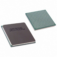
EP3C120F780I7 Altera, EP3C120F780I7 Datasheet - Page 15

EP3C120F780I7
Manufacturer Part Number
EP3C120F780I7
Description
IC CYCLONE III FPGA 120K 780FBGA
Manufacturer
Altera
Series
Cyclone® IIIr
Datasheets
1.EP3C5F256C8N.pdf
(5 pages)
2.EP3C5F256C8N.pdf
(34 pages)
3.EP3C5F256C8N.pdf
(66 pages)
4.EP3C5F256C8N.pdf
(14 pages)
5.EP3C5F256C8N.pdf
(76 pages)
6.EP3C120F780I7.pdf
(274 pages)
Specifications of EP3C120F780I7
Number Of Logic Elements/cells
119088
Number Of Labs/clbs
7443
Total Ram Bits
3981312
Number Of I /o
531
Voltage - Supply
1.15 V ~ 1.25 V
Mounting Type
Surface Mount
Operating Temperature
-40°C ~ 100°C
Package / Case
780-FBGA
Family Name
Cyclone III
Number Of Logic Blocks/elements
119088
# I/os (max)
531
Frequency (max)
437.5MHz
Process Technology
65nm
Operating Supply Voltage (typ)
1.2V
Logic Cells
119088
Ram Bits
3981312
Operating Supply Voltage (min)
1.15V
Operating Supply Voltage (max)
1.25V
Operating Temp Range
-40C to 100C
Operating Temperature Classification
Industrial
Mounting
Surface Mount
Pin Count
780
Package Type
FBGA
For Use With
544-2589 - KIT DEV EMB CYCLONE III EDITION544-2566 - KIT DEV DSP CYCLONE III EDITION544-2444 - KIT DEV CYCLONE III EP3C120
Lead Free Status / RoHS Status
Contains lead / RoHS non-compliant
Number Of Gates
-
Lead Free Status / Rohs Status
Not Compliant
Available stocks
Company
Part Number
Manufacturer
Quantity
Price
Part Number:
EP3C120F780I7
Manufacturer:
ALTERA/阿尔特拉
Quantity:
20 000
Company:
Part Number:
EP3C120F780I7N
Manufacturer:
ALTERA
Quantity:
118
Early System Planning
Planning for On-Chip Debugging
© November 2008 Altera Corporation
f
f
The Quartus II software includes various debugging tools. The following is the list of
debugging tools and their use as well as the requirement for using the tools. Using
these tools in your design flow is optional, but is recommended.
SignalProbe Incremental Routing
The SignalProbe Incremental Routing feature allows you to route internal signals to
I/O pins without affecting the routing of the original design. Starting with a fully
routed design, you can select and route the signals for debugging to either previously
reserved or currently unused I/O pins. To use the SignalProbe feature, you must have
additional I/Os in your device for the signals to be routed to. These I/Os should be
routed out on the board in order for you to be able to probe the signals. You can use
the SignalProbe feature to monitor synchronous or asynchronous signals.
For more information about ways to use the SignalProbe feature for debugging, refer
to the
Handbook.
SignalTap II Embedded Logic Analyzer
The SignalTap II Embedded Logic Analyzer captures and displays real-time behavior
of your FPGA design's internal and I/O signals while the design is running at full
speed, without the need for additional I/O pins or external probes.
You can use the SignalTap II Embedded Logic Analyzer by instantiating the SignalTap
II Logic Analyzer megafunction and includes that in your design or by creating a
SignalTap II Logic Analyzer (.stp) file so that you do not need to modify your design.
The SignalTap II Embedded Logic Analyzer is suitable for capturing synchronous
signals and needs a clock signal from your design to control data acquisition. The
SignalTap II Embedded Logic Analyzer requires JTAG connection and communicates
with the device through an Altera download cable. Additional LEs and the M9K
memory are needed as well.
To minimize changes to your Cyclone III device's performance and reduce
compilation time when you use the SignalTap II Embedded Logic Analyzer,
back-annotate your design and use incremental compilation.
For more information about how to use the SignalTap II Embedded Logic Analyzer
for debugging, refer to the
Analyzer
Logic Analyzer Interface
Logic Analyzer Interface enables you to connect and transmit the internal FPGA
signals to an external logic analyzer or a mixed signal oscilloscope for analysis. You
can use this feature to connect a large set of internal device signals to a small number
of output pins for debugging purposes. This feature functions as a multiplexer and
you can select which of the signal groups to be connected to the output pins for
monitoring on the fly, without the need to recompile the design or reconfigure the
FPGA.
Quick Design Debugging Using SignalProbe
chapter in volume 3 of the Quartus II Handbook.
Design Debugging Using the SignalTap II Embedded Logic
chapter in volume 3 of the Quartus II
Page 15


