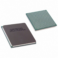
EP3C120F780I7 Altera, EP3C120F780I7 Datasheet - Page 38

EP3C120F780I7
Manufacturer Part Number
EP3C120F780I7
Description
IC CYCLONE III FPGA 120K 780FBGA
Manufacturer
Altera
Series
Cyclone® IIIr
Datasheets
1.EP3C5F256C8N.pdf
(5 pages)
2.EP3C5F256C8N.pdf
(34 pages)
3.EP3C5F256C8N.pdf
(66 pages)
4.EP3C5F256C8N.pdf
(14 pages)
5.EP3C5F256C8N.pdf
(76 pages)
6.EP3C120F780I7.pdf
(274 pages)
Specifications of EP3C120F780I7
Number Of Logic Elements/cells
119088
Number Of Labs/clbs
7443
Total Ram Bits
3981312
Number Of I /o
531
Voltage - Supply
1.15 V ~ 1.25 V
Mounting Type
Surface Mount
Operating Temperature
-40°C ~ 100°C
Package / Case
780-FBGA
Family Name
Cyclone III
Number Of Logic Blocks/elements
119088
# I/os (max)
531
Frequency (max)
437.5MHz
Process Technology
65nm
Operating Supply Voltage (typ)
1.2V
Logic Cells
119088
Ram Bits
3981312
Operating Supply Voltage (min)
1.15V
Operating Supply Voltage (max)
1.25V
Operating Temp Range
-40C to 100C
Operating Temperature Classification
Industrial
Mounting
Surface Mount
Pin Count
780
Package Type
FBGA
For Use With
544-2589 - KIT DEV EMB CYCLONE III EDITION544-2566 - KIT DEV DSP CYCLONE III EDITION544-2444 - KIT DEV CYCLONE III EP3C120
Lead Free Status / RoHS Status
Contains lead / RoHS non-compliant
Number Of Gates
-
Lead Free Status / Rohs Status
Not Compliant
Available stocks
Company
Part Number
Manufacturer
Quantity
Price
Part Number:
EP3C120F780I7
Manufacturer:
ALTERA/阿尔特拉
Quantity:
20 000
Company:
Part Number:
EP3C120F780I7N
Manufacturer:
ALTERA
Quantity:
118
Page 38
Design and Compilation
Clock Power Management
Clock routing power is automatically optimized by the Quartus II software, which
only enables those portions of the clock network that are required to feed downstream
registers. Alternately, you can use clock control blocks to implement the clock enable
signal. When a clock network is powered down, all the logic fed by that clock network
does not toggle, thereby reducing the overall power consumption of the device.
f
For more information about how to use the clock control block, refer to the
altclkctrl
Megafunction User Guide.
Reducing Memory Power Consumption
The key to reducing memory power consumption is to reduce the number of memory
clocking events. This can be achieved through the use of the clock control blocks on
the clock network or on per memory basis through the use of the clock enable signals
on the memory port. The clock enable signal enables the memory only when
necessary and shuts it down for the rest of the time, reducing overall memory. You can
use the Quartus II MegaWizard Plug-In Manager to create the enable signals by
selecting the Clock enable signal option when generating the memory block
function.
Reducing I/O Power
The dynamic power consumed in the I/O buffer is proportional to the load
capacitance, output transition frequency, and output voltage swing. Lower the load
capacitance to reduce dynamic power consumption.
Non-terminated I/O standards such as the LVTTL and LVCMOS have a rail-to-rail
output voltage swing equal to the V
supply voltage. Use lower voltage I/O
CCIO
standard to reduce dynamic power. For high speed applications, use
voltage-reference I/O standards, such as the SSTL. The output voltage swings by an
amount smaller than V
around the reference voltage, so dynamic power is lower
CCIO
than that of LVTTL or LVCMOS under the same conditions.
However, voltage-reference I/O standards dissipate significant static power because
current is constantly driven into the termination network. Use the lowest drive
strength that meets your speed and waveform requirements to minimize static power.
On the contrary, LVTTL and LVCMOS consume little static power.
1
Note that the power dissipated in the external termination network is not included in
the EPE or PowerPlay Power Analyzer calculations. Make sure that you include it
separately in your system power calculations.
Pipelining and Retiming
A design that has many glitches consumes more power because of faster switching
activity. Pipelining by inserting flip flops into long combinational paths can reduce
design glitches. Flip flops do not allow glitches to propagate through combinational
paths, resulting in reduced power dissipation in combinational logic. However, if
there are not many glitches in your design, pipelining may increase power
consumption due to the addition of unnecessary registers.
© November 2008 Altera Corporation


