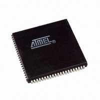
AT94K10AL-25AJI Atmel, AT94K10AL-25AJI Datasheet - Page 14

AT94K10AL-25AJI
Manufacturer Part Number
AT94K10AL-25AJI
Description
IC FPSLIC 10K GATE 25MHZ 84PLCC
Manufacturer
Atmel
Series
FPSLIC®r
Specifications of AT94K10AL-25AJI
Core Type
8-bit AVR
Speed
25MHz
Interface
I²C, UART
Program Sram Bytes
20K-32K
Fpga Sram
4kb
Data Sram Bytes
4K ~ 16K
Fpga Core Cells
576
Fpga Gates
10K
Fpga Registers
846
Voltage - Supply
3 V ~ 3.6 V
Mounting Type
Surface Mount
Operating Temperature
-40°C ~ 85°C
Package / Case
84-PLCC
For Use With
ATSTK594 - BOARD FPSLIC DAUGHTER FOR STK500
Lead Free Status / RoHS Status
Contains lead / RoHS non-compliant
Eeprom Size
-
Available stocks
Company
Part Number
Manufacturer
Quantity
Price
- Current page: 14 of 204
- Download datasheet (4Mb)
2.10
14
Clocking and Set/Reset
AT94KAL Series FPSLIC
Six of the eight dedicated Global Clock buses (1, 2, 3, 4, 7 and 8) are connected to a dual-use
Global Clock pin. In addition, two Global Clock buses (5 and 6) are driven from clock signals
generated within the AVR microcontroller core, see
An FPGA core internal signal can be placed on any Global Clock bus by routing that signal to a
Global Clock access point in the corners of the embedded core. Each column of the array has a
Column Clock selected from one of the eight Global Clock buses. The left edge Column Clock
mux has two additional inputs from dual-use pins FCK1, see
fast clocking to left-side I/O. Each sector column of four cells can be clocked from a (Plane 4)
express bus or from the Column Clock. Clocking to the 4 cells of a sector can be disabled. The
Plane 4 express bus used for clocking is half length at the array edge. The clock provided to
each sector column of four cells can be either inverted or not inverted. The register in each cell is
triggered on a rising clock edge. On power-up, constant “0” is provided to each register’s clock
pins. A dedicated Global Set/Reset bus, see
except those used for clocking, Global or Fast. An internal signal can be placed on the Global
Set/Reset bus by routing that signal to the pad programmed as the Global Set/Reset input. Glo-
bal Set/Reset is distributed to each column of the array. Each sector column of four cells can be
Set/Reset by a (Plane 5) express bus or by the Global Set/Reset. The Plane 5 express bus used
for Set/Reset is half length at array edge. The Set/Reset provided to each sector column of four
cells can be either inverted or not inverted. The function of the Set/Reset input of a register
(either Set or Reset) is determined by a configuration bit for each cell. The Set/Reset input of a
register is Active Low (logic 0). Setting or resetting of a register is asynchronous. On power-up, a
logic 1 (High) is provided by each register, i.e., all registers are set at power-up.
Figure 2-9.
CORE GCK6
TO FPGA
FPGA Clocks from AVR
CORE GCK5
TO FPGA
GCK6
AVR SYSTEM
(AVR CLK)
Figure
CLOCK
AVR SYSTEM CLOCK (AVR CLK)
TIMER OSC TOSC1 (AS2 SET IN ASSR)
WATCHDOG CLOCK
"1"
Figure
2-7, can be driven by any USER I/O pad,
2-9.
Figure
2-6, and FCK2 to provide
1138I–FPSLI–1/08
Related parts for AT94K10AL-25AJI
Image
Part Number
Description
Manufacturer
Datasheet
Request
R

Part Number:
Description:
Manufacturer:
Atmel
Datasheet:

Part Number:
Description:
IC FPSLIC 10K GATE 25MHZ 84PLCC
Manufacturer:
Atmel
Datasheet:

Part Number:
Description:
IC FPSLIC 10K GATE 25MHZ 100TQFP
Manufacturer:
Atmel
Datasheet:

Part Number:
Description:
IC FPSLIC 10K GATE 25MHZ 100TQFP
Manufacturer:
Atmel
Datasheet:

Part Number:
Description:
IC FPSLIC 10K GATE 25MHZ 144LQFP
Manufacturer:
Atmel
Datasheet:

Part Number:
Description:
IC FPSLIC 10K GATE 25MHZ 208PQFP
Manufacturer:
Atmel
Datasheet:

Part Number:
Description:
Manufacturer:
Atmel
Datasheet:

Part Number:
Description:
At94k05al 5k - 40k Gates Of At40k Fpga With 8-bit Microcontroller, Up To 36k Bytes Of Sram And On-chip Jtag Ice
Manufacturer:
ATMEL Corporation
Datasheet:

Part Number:
Description:
FPGA - Field Programmable Gate Array FPSLIC 10K GATE 8B 8B AVR 25MHZ TEMP
Manufacturer:
Atmel

Part Number:
Description:
FPGA - Field Programmable Gate Array ASICS
Manufacturer:
Atmel

Part Number:
Description:
FPGA - Field Programmable Gate Array FPSLIC 10K GATE 8B 8B AVR 25MHZ TEMP
Manufacturer:
Atmel

Part Number:
Description:
DEV KIT FOR AVR/AVR32
Manufacturer:
Atmel
Datasheet:

Part Number:
Description:
INTERVAL AND WIPE/WASH WIPER CONTROL IC WITH DELAY
Manufacturer:
ATMEL Corporation
Datasheet:

Part Number:
Description:
Low-Voltage Voice-Switched IC for Hands-Free Operation
Manufacturer:
ATMEL Corporation
Datasheet:


