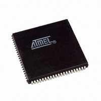
AT94K10AL-25AJI Atmel, AT94K10AL-25AJI Datasheet - Page 31

AT94K10AL-25AJI
Manufacturer Part Number
AT94K10AL-25AJI
Description
IC FPSLIC 10K GATE 25MHZ 84PLCC
Manufacturer
Atmel
Series
FPSLIC®r
Specifications of AT94K10AL-25AJI
Core Type
8-bit AVR
Speed
25MHz
Interface
I²C, UART
Program Sram Bytes
20K-32K
Fpga Sram
4kb
Data Sram Bytes
4K ~ 16K
Fpga Core Cells
576
Fpga Gates
10K
Fpga Registers
846
Voltage - Supply
3 V ~ 3.6 V
Mounting Type
Surface Mount
Operating Temperature
-40°C ~ 85°C
Package / Case
84-PLCC
For Use With
ATSTK594 - BOARD FPSLIC DAUGHTER FOR STK500
Lead Free Status / RoHS Status
Contains lead / RoHS non-compliant
Eeprom Size
-
Available stocks
Company
Part Number
Manufacturer
Quantity
Price
- Current page: 31 of 204
- Download datasheet (4Mb)
1138I–FPSLI–1/08
Table 3-7.
Bit
SCR5
SCR6
SCR7 - SCR12
SCR13
SCR14 - SCR15
SCR16 - SCR23
SCR24 - SCR25
SCR26
SCR27
SCR28 - SCR29
SCR30
FPSLIC System Control Register (Continued)
Description
Reserved
0 = OTS Disabled
1 = OTS Enabled
Setting SCR6 makes the OTS (output tri-state) pin an input which controls the
global tri-state control for all user I/O. This junction allows the user at any time to
tristate all user I/O and isolate the chip.
Reserved
0 = CCLK Normal Operation
1 = CCLK Continues After Configuration.
Setting bit SCR13 allows the CCLK pin to continue to run after configuration
download is completed. This bit is valid for Master mode, mode 0 only. The CCLK
is not available internally on the device. If it is required in the design, it must be
connected to another device I/O.
Reserved
0 = GCK 0:7 Always Enabled
1 = GCK 0:7 Disabled During Internal and External Configuration Download.
Setting SCR16:SCR23 allows the user to disable the input buffers driving the
global clocks. The clock buffers are enabled and disabled synchronously with the
rising edge of the respective GCK signal, and stop in a High “1” state. Setting one
of these bits disables the appropriate GCK input buffer only and has no effect on
the connection from the input buffer to the FPGA array.
0 = FCK 0:1 Always Enabled
1 = FCK 0:1 Disabled During Internal and External Configuration Download.
Setting SCR24:SCR25 allows the user to disable the input buffers driving the fast
clocks. The clock buffers are enabled and disabled synchronously with the rising
edge of the respective FCK signal, and stop in a High “1” state. Setting one of
these bits disables the appropriate FCK input buffer only and has no effect on the
connection from the input buffer to the FPGA array.
0 = Disable On-chip Debugger
1 = Enable On-chip Debugger.
JTAG Enable, SCR27, must also be set (one) and the configuration memory
lockout, SCR4, must be clear (zero) for the user to have access to internal scan
chains.
0 = Disable TAP at user FPGA I/O Ports
1 = Enable TAP at user FPGA I/O Ports.
Device ID scan chain and AVR I/O boundary scan chain are available. The user
must set (one) the On-chip Debug Enable, SCR26, and must keep the
configuration memory lockout, SCR4, clear (zero) for the user to have access to
internal scan chains.
Reserved
0 = Global Set/Reset Normal
1 = Global Set/Reset Active (Low) During Internal and External Configuration
Download.
SCR30 allows the Global set/reset to hold the core DFFs in reset during any
configuration download. The Global set/reset net is released at the end of
configuration download on the rising edge of CON, if set.
AT94KAL Series FPSLIC
31
Related parts for AT94K10AL-25AJI
Image
Part Number
Description
Manufacturer
Datasheet
Request
R

Part Number:
Description:
Manufacturer:
Atmel
Datasheet:

Part Number:
Description:
IC FPSLIC 10K GATE 25MHZ 84PLCC
Manufacturer:
Atmel
Datasheet:

Part Number:
Description:
IC FPSLIC 10K GATE 25MHZ 100TQFP
Manufacturer:
Atmel
Datasheet:

Part Number:
Description:
IC FPSLIC 10K GATE 25MHZ 100TQFP
Manufacturer:
Atmel
Datasheet:

Part Number:
Description:
IC FPSLIC 10K GATE 25MHZ 144LQFP
Manufacturer:
Atmel
Datasheet:

Part Number:
Description:
IC FPSLIC 10K GATE 25MHZ 208PQFP
Manufacturer:
Atmel
Datasheet:

Part Number:
Description:
Manufacturer:
Atmel
Datasheet:

Part Number:
Description:
At94k05al 5k - 40k Gates Of At40k Fpga With 8-bit Microcontroller, Up To 36k Bytes Of Sram And On-chip Jtag Ice
Manufacturer:
ATMEL Corporation
Datasheet:

Part Number:
Description:
FPGA - Field Programmable Gate Array FPSLIC 10K GATE 8B 8B AVR 25MHZ TEMP
Manufacturer:
Atmel

Part Number:
Description:
FPGA - Field Programmable Gate Array ASICS
Manufacturer:
Atmel

Part Number:
Description:
FPGA - Field Programmable Gate Array FPSLIC 10K GATE 8B 8B AVR 25MHZ TEMP
Manufacturer:
Atmel

Part Number:
Description:
DEV KIT FOR AVR/AVR32
Manufacturer:
Atmel
Datasheet:

Part Number:
Description:
INTERVAL AND WIPE/WASH WIPER CONTROL IC WITH DELAY
Manufacturer:
ATMEL Corporation
Datasheet:

Part Number:
Description:
Low-Voltage Voice-Switched IC for Hands-Free Operation
Manufacturer:
ATMEL Corporation
Datasheet:


