MPC8379EVRAJF Freescale Semiconductor, MPC8379EVRAJF Datasheet - Page 115
MPC8379EVRAJF
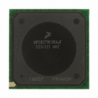
Manufacturer Part Number
MPC8379EVRAJF
Description
MPU PWRQUICC II 533MHZ 689TEPBGA
Manufacturer
Freescale Semiconductor
Series
PowerQUICC II PROr
Datasheets
1.MPC8377EVRAGD.pdf
(126 pages)
2.MPC8377EVRAGD.pdf
(2 pages)
3.MPC8379VRAGD.pdf
(116 pages)
Specifications of MPC8379EVRAJF
Processor Type
MPC83xx PowerQUICC II Pro 32-Bit
Speed
533MHz
Voltage
1V
Mounting Type
Surface Mount
Package / Case
689-TePBGA II
Maximum Clock Frequency
533 MHz
Operating Supply Voltage
1.8 V to 2.5 V
Maximum Operating Temperature
+ 105 C
Mounting Style
SMD/SMT
I/o Voltage
1.8 V, 2.5 V, 3.3 V
Minimum Operating Temperature
0 C
Core Size
32 Bit
Program Memory Size
64KB
Cpu Speed
533MHz
Embedded Interface Type
DUART, HSSI, I2C, IPIC, JTAG, SPI, USB
Digital Ic Case Style
BGA
No. Of Pins
689
Rohs Compliant
Yes
For Use With
MPC8377E-RDBA - BOARD REF DES MPC8377 REV 2.1MPC8377E-MDS-PB - BOARD MODULAR DEV SYSTEM
Lead Free Status / RoHS Status
Lead free / RoHS Compliant
Features
-
Lead Free Status / Rohs Status
Lead free / RoHS Compliant
Available stocks
Company
Part Number
Manufacturer
Quantity
Price
Company:

Part Number:
MPC8379EVRAJF
Manufacturer:
Freescale Semiconductor
Quantity:
135
Company:
Part Number:
MPC8379EVRAJF
Manufacturer:
Freescale Semiconductor
Quantity:
10 000


Freescale Semiconductor
Revision
1
2
0
10/2009 • In
02/2009 • In
12/2008 Initial public release.
Date
• In
• In
• In
• In
• In
• In
• In
• In
• In
• In
• In
• In
• In
• In
• In
• In
• In
• In
• In
• In
• Updated part numbering information in AF column in
• In
MPC8379E PowerQUICC II Pro Processor Hardware Specifications, Rev. 4
800/400 MHz to 4.3 W.
Application at T
at T
and DDR2 to 600 and 400 μA, respectively. Also, updated Note 1 and added Note 2.
“Min” and “Max”. Footnote 2 updated to state “T is the MCK clock period”.
DDR2 SDRAM Output AC Timing Specifications,” clarified that the frequency parameters are data rates.
Specifications,” corrected titles from “Transmitter” to “Receiver”.
to VDD pin.
range to 125–200.
respectively.
rows for SerDes. In addition, changed 666 to 667 MHz.
changed 666 to 667 MHz.
DDR2 SDRAM Output AC Timing Specifications,” and
footnote to references to MVREF, MDQ, and MDQS, referencing AN3665, MPC837xE Design Checklist.
footnote 10 and added footnote 15.
addition, modified extended temperature information in notes 1 and 4.
Section 19.2, “SPI AC Timing Specifications,”
Table
Table
Table
Table
Table
Table
Table
Table
Table
Table
Table
Table
Table
Table
Table
Table
Table
Table
Table
Table
Table
Table
j
= 65°C (W)”.
13, “DDR2 SDRAM DC Electrical Characteristics for GV
3, “Recommended Operating Conditions,” added “Operating temperature range” values.
5, “MPC8377EMPC8378EMPC8379E Power Dissipation
5, “MPC8377EMPC8378EMPC8379E Power Dissipation
5, “MPC8377EMPC8378EMPC8379E Power Dissipation
11, removed overbar from CFG_CLKIN_DIV.
17, “Current Draw Characteristics for MV
20, “DDR1 and DDR2 SDRAM Input AC Timing Specifications,” column headings renamed to
20, “DDR1 and DDR2 SDRAM Input AC Timing Specifications,” and
29, “RMII Transmit AC Timing Specifications,” updated t
57, Gen 1i/1.5G Transmitter AC Specifications,” and
69, “TePBGA II Pinout
71, “Operating Frequencies for TePBGA
76, “e300 Core PLL Configuration,” added 3.5:1 and 4:1 core_clk: csb_clk ratio options.
77, “Example Clock Frequency Combinations,” updated column heading to “DDR data rate” .
3, “Recommended Operating Conditions,” added two new rows for 800 MHz, and created two
5, “MPC8377EMPC8378EMPC8379E Power Dissipation
21, updated t
69, “TePBGA II Pinout Listing,” added footnote to USBDR_STP_SUSPEND and modified
71, “Operating Frequencies for TePBGA II,” changed 667 to 800 MHz for core_clk.
77, “Example Clock Frequency Combinations,” added 800 MHz cells for e300 core.
82, “Available Parts (Core/DDR Data Rate),” added new row for 800/400 MHz.
Table 84. Document Revision History (continued)
j
= 65°C (W)”.
DDKHCX
minimum value for 333 MHz to 2.40.
Listing,”
Substantive Change(s)
removed pin THERM0; it is now Reserved. Also added 1.05 V
corrected t
II,”
REF
corrected “DDR2 memory bus frequency (MCK)”
,” updated I
Table
Table
NIKHOX
81, “Part Numbering Nomenclature.” In
69, “TePBGA II Pinout Listing,” added
Table
MVREF
RMTDX
DD
and t
1
1
1
1
,” corrected maximal application for
,” added a column for “Sleep Power
,” added Notes 4 and 5. In addition,
(typ) = 1.8 V,”
,” added a column for “Typical
59, Gen 2i/3G Transmitter AC
I to 2.0 ns.
NEKHOX
maximum value for both DDR1
Document Revision History
Table
to t
Table
NIKHOV
21, “DDR1 and
21, “DDR1 and
and t
NEKHOV
115
,
Related parts for MPC8379EVRAJF
Image
Part Number
Description
Manufacturer
Datasheet
Request
R

Part Number:
Description:
BOARD REF DESIGN MPC8379E
Manufacturer:
Freescale Semiconductor
Datasheet:

Part Number:
Description:
BOARD REFERENCE FOR MPC837
Manufacturer:
Freescale Semiconductor
Datasheet:
Part Number:
Description:
BOARD PROCESSOR FOR MDS S
Manufacturer:
Freescale Semiconductor
Datasheet:

Part Number:
Description:
Powerquicc Ii Pro Processor Hardware Specifications
Manufacturer:
Freescale Semiconductor, Inc
Datasheet:

Part Number:
Description:
BOARD REF DES MPC8377 REV 2.1
Manufacturer:
Freescale Semiconductor
Datasheet:
Part Number:
Description:
Manufacturer:
Freescale Semiconductor, Inc
Datasheet:
Part Number:
Description:
Manufacturer:
Freescale Semiconductor, Inc
Datasheet:
Part Number:
Description:
Manufacturer:
Freescale Semiconductor, Inc
Datasheet:
Part Number:
Description:
Manufacturer:
Freescale Semiconductor, Inc
Datasheet:
Part Number:
Description:
Manufacturer:
Freescale Semiconductor, Inc
Datasheet:
Part Number:
Description:
Manufacturer:
Freescale Semiconductor, Inc
Datasheet:
Part Number:
Description:
Manufacturer:
Freescale Semiconductor, Inc
Datasheet:
Part Number:
Description:
Manufacturer:
Freescale Semiconductor, Inc
Datasheet:
Part Number:
Description:
Manufacturer:
Freescale Semiconductor, Inc
Datasheet:
Part Number:
Description:
Manufacturer:
Freescale Semiconductor, Inc
Datasheet: