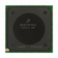
MPC8379EVRAJF Freescale Semiconductor, MPC8379EVRAJF Datasheet
MPC8379EVRAJF
Specifications of MPC8379EVRAJF
Available stocks


Related parts for MPC8379EVRAJF


MPC8379EVRAJF Summary of contents
Page 1
... Mbps Ethernet interfaces, a DDR1/DDR2 SDRAM memory controller, a flexible, a 32-bit local bus controller, a 32-bit PCI controller, an optional dedicated security engine, a USB © Freescale Semiconductor, Inc., 2008–2010. All rights reserved. Document Number: MPC8377EEC Rev. 4, 11/2010 Contents 1 ...
Page 2
... Core 32-Kbyte 32-Kbyte D-Cache I-Cache USB 2.0 eTSEC eTSEC RGMII, RMII, RGMII, RMII, Device RTBI, MII RTBI, MII 2 C controllers, a 4-channel DMA Figure 1he block DDR1/DDR2 Enhanced SDRAM Local Bus Controller SD/MMC PCI SATA Controller Express x1 x2 PHY PHY Freescale Semiconductor ...
Page 3
... Enhanced host controller interface (EHCI) compatible • Supports high-speed (480 Mbps), full-speed (12 Mbps), and low-speed (1.5 Mbps) operation; low-speed operation is supported only in host mode • Supports UTMI + low pin interface (ULPI) MPC8377E PowerQUICC II Pro Processor Hardware Specifications, Rev. 4 Freescale Semiconductor MPC8377E MPC8378E ...
Page 4
... The device provides an integrated four-channel DMA controller with the following features: • Allows chaining (both extended and direct) through local memory-mapped chain descriptors (accessible by local masters) • Supports misaligned transfers MPC8377E PowerQUICC II Pro Processor Hardware Specifications, Rev DUART, Enhanced Local Bus Controller Freescale Semiconductor ...
Page 5
... Single 32-bit data PCI interface operates MHz • PCI 3.3-V compatible (not 5-V compatible) • Support for host and agent modes • On-chip arbitration, supporting 5 external masters on PCI • Selectable hardware-enforced coherency MPC8377E PowerQUICC II Pro Processor Hardware Specifications, Rev. 4 Freescale Semiconductor Overview 5 ...
Page 6
... Interrupt driven • Power management support • Error handling and diagnostic features — Far end/near end loopback — Failed CRC error reporting — Increased ALIGN insertion rates • Scrambling and CONT override MPC8377E PowerQUICC II Pro Processor Hardware Specifications, Rev Freescale Semiconductor ...
Page 7
... PLL supply voltage (e300 core, eLBC, and system) DDR1 and DDR2 DRAM I/O voltage Three-speed Ethernet I/O, MII management voltage PCI, DUART, system control and power management, I JTAG I/O voltage Local bus SerDes MPC8377E PowerQUICC II Pro Processor Hardware Specifications, Rev. 4 Freescale Semiconductor Table 2. Absolute Maximum Ratings Symbol ...
Page 8
... Figure 2. Table 3 Recommended Symbol Unit Value V 1.0 ± 1.05 ± 1.0 ± 1.05 ± 2.5 V ± 125 1.8 V ± [1,2] 3.3 V ± 165 2.5 V ± 125 mV OV 3.3 V ± 165 Freescale Semiconductor Notes — — are Notes — 1 ...
Page 9
... Please note that with the PCI overshoot allowed (as specified above), the device does not fully comply with the maximum AC ratings and device protection guideline outlined in the PCI Rev. 2.3 Specification (Section 4.2.2.3). Figure 2. Overshoot/Undershoot Voltage for GV MPC8377E PowerQUICC II Pro Processor Hardware Specifications, Rev. 4 Freescale Semiconductor up to 667 MHz L[1,2]_nV 800 MHz commerical ...
Page 10
... I/O Voltage (GVDD, LVDD, and OVDD) Core Voltage (VDD Figure 3. Power-Up Sequencing Example Supply Voltage 45 LBV = 2 LBV = 2 and AV ) before the I/O voltages and DD and AV must reach 90% of their DD Figure 3. I/O voltage AVDD Freescale Semiconductor ...
Page 11
... MHz, and running a Dhrystone benchmark application. 4 Maximum power is based on a voltage 800 MHz, worst case process, and running an artificial smoke test. MPC8377E PowerQUICC II Pro Processor Hardware Specifications, Rev. 4 Freescale Semiconductor ) should follow the same timing as the core supply DD Table 5. MPC8377E Power Dissipation Sleep Power ...
Page 12
... L[1,2]_nV DD Unit Comments (1.0 V) — W — — W — W — W — W — W — W — W — W — W — W — — W — W — — W — W — W — W Freescale Semiconductor ...
Page 13
... Table 7. CLKIN DC Electrical Characteristics Parameter Input high voltage Input low voltage CLKIN Input current PCI_CLK Input current OV Note PCI agent mode, this specification does not comply with PCI 2.3 Specification. MPC8377E PowerQUICC II Pro Processor Hardware Specifications, Rev. 4 Freescale Semiconductor GV /LBV (2.5 V) (3.3 V) (3.3 V) — ...
Page 14
... Typical Max Unit 125 — MHz 8 — ns — ns 0.75 1.0 — — ±150 ps = 2.5 V and from 0.6 and 2.7 V for DD for the duty cycle for 10Base-T and 100Base-T Freescale Semiconductor Notes 1, 6 — Notes — — ...
Page 15
... Input setup time for POR config signals (CFG_RESET_SOURCE[0:3], CFG_CLKIN_DIV, and CFG_LBMUX) with respect to negation of PORESET when the device is in PCI agent mode Input hold time for POR config signals with respect to negation of HRESET MPC8377E PowerQUICC II Pro Processor Hardware Specifications, Rev. 4 Freescale Semiconductor Symbol Condition V — ...
Page 16
... GV MV REF – 0.04 TT REF 0.140 IH REF V –0 – –13.4 OH Min Max Unit Notes — — PCI_SYNC_IN Unit Notes μs — (typ (typ Max Unit Notes 1. 0.51 × 0. REF GV + 0.3 V — – 0.140 V — REF μ — mA — Freescale Semiconductor ...
Page 17
... MV . This rail should track variations in the DC level of MV REF 4 Output leakage is measured with all outputs disabled See AN3665, “MPC837xE Design Checklist,” for proper DDR termination. MPC8377E PowerQUICC II Pro Processor Hardware Specifications, Rev. 4 Freescale Semiconductor Symbol Min I 13 all times and to track GV DC variations as measured at the receiver ...
Page 18
... V DD Max Unit — 0 /2, V (peak-to-peak) = 0.2 V. OUT DD OUT REF Typ Max Unit μA 250 600 150 400 VDD(typ) G Max MV – 0.25 REF + 0.25 — (typ Max MV – 0.31 REF + 0.31 — Freescale Semiconductor Notes 1 1 Note Unit V V Unit V V ...
Page 19
... MHz data rate MCSn output hold with respect to MCK 400 MHz data rate 333 MHz data rate 266 MHz data rate 200 MHz data rate MCK to MDQS skew MPC8377E PowerQUICC II Pro Processor Hardware Specifications, Rev. 4 Freescale Semiconductor Symbol Min t CISKEW –500 –750 –750 = ± ...
Page 20
... DDR timing (DD) for the time t DDKLDX Max Unit Notes — — — — — — — — –0.5 × 0 MCK 0 for memory clock reference MCK describes the DDR timing (DD) DDKHMH can be modified through control DDKHMH follows the symbol DDKHMP Freescale Semiconductor ...
Page 21
... Figure 5 shows the DDR1 and DDR2 SDRAM output timing diagram. MCK[n] MCK[n] ADDR/CMD Write A0 MDQS[n] MDQ[x] Figure 5. DDR1 and DDR2 SDRAM Output Timing Diagram MPC8377E PowerQUICC II Pro Processor Hardware Specifications, Rev. 4 Freescale Semiconductor MCK[n] MCK[n] t MCK t DDKHMHmax) = 0.6 ns MDQS t DDKHMH(min) = –0.6 ns MDQS Figure 4 ...
Page 22
... IN symbol referenced in Table IN Table 23. DUART AC Timing Specifications th sampled 0 after the 1-to-0 transition of the start bit. Subsequent bit values are GVDD Ω Max OV + 0.3 DD 0.8 — 0.2 ±30 2. Value Unit 256 baud > 1,000,000 baud 16 — Freescale Semiconductor Unit μA Notes — ...
Page 23
... IN DD2 Input low current (V = GND) IN Note supports eTSEC 1. DD1 LV supports eTSEC 2. DD2 MPC8377E PowerQUICC II Pro Processor Hardware Specifications, Rev. 4 Freescale Semiconductor Ethernet: Enhanced Three-Speed Ethernet (eTSEC) Table 25 are based on a 2.5 V CMOS interface voltage as Symbol Min LV 3.13 DD1 LV DD2 V 2.40 LV /LV ...
Page 24
... Symbol t MTX t MTX t t MTXH/ MTX t MTKHDX Max Unit Notes 2. /LV + 0.3 V DD1 DD2 0. /LV + 0.3 V DD1 DD2 0.70 V μA –20 μA — Min Typical Max — 400 — — 40 — 35 — Freescale Semiconductor 1, 2 — — — — — Unit ...
Page 25
... Input low voltage Input high voltage RX_CLK clock period 10 Mbps RX_CLK clock period 100 Mbps RX_CLK duty cycle RXD[3:0], RX_DV, RX_ER setup time to RX_CLK RXD[3:0], RX_DV, RX_ER hold time to RX_CLK MPC8377E PowerQUICC II Pro Processor Hardware Specifications, Rev. 4 Freescale Semiconductor of 3.3 V ± 5 Symbol t MTXR t ...
Page 26
... Symbol Min t –600 SKRGT t 1.0 SKRGT t 7.2 RGT Min Typical Max 1.0 — 4.0 1.0 — 4.0 symbolizes MII MRDVKH clock reference MRX LVDD Ω MRXR t MRDXKL Typical Max Unit 0 600 ps — 2.8 ns 8.0 8.8 ns Freescale Semiconductor Unit ns ns Notes — ...
Page 27
... This symbol represents the external EC_GTX_CLK125 and does not follow the original signal naming convention. Figure 10 provides the AC test load for eTSEC. Output MPC8377E PowerQUICC II Pro Processor Hardware Specifications, Rev. 4 Freescale Semiconductor Ethernet: Enhanced Three-Speed Ethernet (eTSEC) of 2.5 V ± 5 Symbol Min ...
Page 28
... TXD[8:5] TXD[3:0] TXD[7:4] TXD[9] TXD[4] TXEN TXERR RXD[8:5] RXD[3:0] RXD[7:4] t SKRGT RXD[4] RXD[9] RXDV RXERR Table 29. of 3.3 V ± 5 Symbol t RMT t RMTH t RMTJ t RMTR t RGT t SKRGT t SKRGT Min Typical Max 15.0 20.0 25 — — 250 1.0 — 2.0 Freescale Semiconductor Unit ...
Page 29
... DD Input high voltage at 3 REF_CLK clock period REF_CLK duty cycle REF_CLK peak-to-peak jitter Rise time REF_CLK (20%–80%) Fall time REF_CLK (80%–20%) MPC8377E PowerQUICC II Pro Processor Hardware Specifications, Rev. 4 Freescale Semiconductor of 3.3 V ± 5 Symbol t RMTF t RMTDX (first two letters of functional block)(signal)(state) (reference)(state) for outputs ...
Page 30
... RMRF RMRH Valid Data t RMRDV Figure 14. RMII Receive AC Timing Diagram = 50 Ω Figure 15. eTSEC AC Test Load 1 Min Typical Max 4.0 — — 2.0 — — symbolizes MII MRDVKH clock reference MRX LVDD Ω RMRR t RMRDX LVDD Ω Freescale Semiconductor Unit ns ns ...
Page 31
... Table 33. MII Management AC Timing Specifications Parameter MDC frequency MDC period MDC clock pulse width high MDC to MDIO valid MDC to MDIO delay MDIO to MDC setup time MDIO to MDC hold time MPC8377E PowerQUICC II Pro Processor Hardware Specifications, Rev. 4 Freescale Semiconductor Table 31 and Conditions Symbol — LV DD1 LV = Min ...
Page 32
... MDC clock reference (K) going to the high (H) state or setup time. For rise and fall times, the t MDC t t MDCH MDCF MDDVKH t t MDDXKH t MDKHDX Max Unit — — symbolizes MDKHDX t MDCR Freescale Semiconductor Notes 4 4 ...
Page 33
... For active/float timing measurements, the high impedance or off state is defined to be when the total current delivered through the component pin is less than or equal to that of the leakage current specification. MPC8377E PowerQUICC II Pro Processor Hardware Specifications, Rev. 4 Freescale Semiconductor Table 34. USB DC Electrical Characteristics Symbol ...
Page 34
... DC electrical characteristics for the local bus interface Conditions Symbol — LBV LBV = Min 4.0 mA LBV = Min V DD — — V — — LBV GND Ω USIXKH = 3 Min Max 3.135 3.465 DD 2.40 — OH — 0.50 OL 2.0 LBV + 0 –0.3 0. — –30 — IL Freescale Semiconductor Unit μA μA ...
Page 35
... LALE output fall to LAD output transition (LATCH hold time) LALE output fall to LAD output transition (LATCH hold time) Local bus clock to LALE rise Local bus clock to output valid (except LALE) MPC8377E PowerQUICC II Pro Processor Hardware Specifications, Rev. 4 Freescale Semiconductor = 2 Conditions — ...
Page 36
... LBK /2 and the 0.4 × LBV the rising/falling edge of LSYNC_IN to 0.5 × LBV DD Min Max Unit — 3 — ns symbolizes local bus LBIXKH1 clock reference (K) goes high (H), in this case for of the signal in question the signal in question. DD Freescale Semiconductor Notes ...
Page 37
... For purposes of active/float timing measurements, the Hi-Z or off state is defined to be when the total current delivered through the component pin is less than or equal to the leakage current specification. Figure 19 provides the AC test load for the local bus. Output MPC8377E PowerQUICC II Pro Processor Hardware Specifications, Rev. 4 Freescale Semiconductor 1 Symbol t LBK t ...
Page 38
... LAD[0:31]/LDP[0:3] Output (Address) Signal: LAD[0:31] LALE Figure 20. Local Bus Signals, Non-special Signals Only (PLL Enable Mode) MPC8377E PowerQUICC II Pro Processor Hardware Specifications, Rev LBIVKH t LBIVKH t LBKHOX t LBKHOV t LBKHOZ t LBKHOX t LBKHOV t LBKHOZ t LBKHOX t LBKHOV t t LBOTOT LBKHLR t LBIXKH t LBIXKH Freescale Semiconductor ...
Page 39
... LGTA Output Signals: LSDA10/LSDWE/LSDRAS/ LSDCAS/LSDDQM[0:3] LA[27:31]/LBCTL/LBCKE/LOE Output (Data) Signals: LAD[0:31]/LDP[0:3] Output (Address) Signal: LAD[0:31] LALE Figure 21. Local Bus Signals, Non-special Signals Only (PLL Bypass Mode) MPC8377E PowerQUICC II Pro Processor Hardware Specifications, Rev. 4 Freescale Semiconductor t LBIVKH t LBKHOV t LBKHOZ t LBKHOV t LBKHOZ t ...
Page 40
... Output (Data) Signals: LAD[0:31]/LDP[0:3] Output (Address) Signal: LAD[0:31] Figure 22. Local Bus Signals, GPCM/UPM Signals for LCRR[CLKDIV (PLL Enable Mode) MPC8377E PowerQUICC II Pro Processor Hardware Specifications, Rev LBKHOV LBKHOX t LBIVKH t LBIVKH t LBKHOX t LBKHOV t LBKHOZ t LBKHOX t LBKHOV t LBKHOZ t LBKHOX t LBKHOV t LBIXKH t LBIXKH Freescale Semiconductor ...
Page 41
... LAD[0:31]/LDP[0:3] UPM Mode Output Signals: LCS[0:7]/LBS[0:1]/LGPL[0:5] Output (Data) Signals: LAD[0:31]/LDP[0:3] Output (Address) Signal: LAD[0:31] Figure 23. Local Bus Signals, GPCM/UPM Signals for LCRR[CLKDIV (PLL Bypass Mode) MPC8377E PowerQUICC II Pro Processor Hardware Specifications, Rev. 4 Freescale Semiconductor t LBKHOZ t LBKHOV t LBIVKH t t ...
Page 42
... Output (Data) Signals: LAD[0:31]/LDP[0:3] Output (Address) Signal: LAD[0:31] Figure 24. Local Bus Signals, GPCM/UPM Signals for LCRR[CLKDIV (PLL Enable Mode) MPC8377E PowerQUICC II Pro Processor Hardware Specifications, Rev LBKHOZ t LBKHOV t LBIVKH t LBIVKH t LBKHOX t LBKHOV t LBKHOZ t LBKHOX t LBKHOV t LBKHOZ t LBKHOX t LBKHOV t LBIXKH t LBIXKH Freescale Semiconductor ...
Page 43
... SD_DAT[0:3]/CMD as outputs and sample the SD_DAT[0:3] as inputs. This behavior is true for both full- and high-speed modes. Note that this is a non-standard implementation, as the SD card specification assumes that in high-speed mode, data is driven at the rising edge of the clock. MPC8377E PowerQUICC II Pro Processor Hardware Specifications, Rev. 4 Freescale Semiconductor Enhanced Secure Digital Host Controller (eSDHC) t LBKHOZ t ...
Page 44
... SFSCKR t SFSCKF t SFSIVKH Min Max 0.625 × 0 0.25 × OV –0.3 DD — ±30 0.75 × OV — DD 0.125 × OV — DD Figure 27 Min Max Unit 0 25 MHz 40 — 400 KHz 15 — — ns — — ns Freescale Semiconductor Unit V V μ and Notes — — — ...
Page 45
... For reference only, according to the SD card specifications. 4 Average, for reference only. Figure 26 provides the eSDHC clock input timing diagram. eSDHC External Clock operational mode Figure 26. eSDHC Clock Input Timing Diagram MPC8377E PowerQUICC II Pro Processor Hardware Specifications, Rev. 4 Freescale Semiconductor = 3.3 V ± 165 mV Symbol t SFSIXKH t INT_CLK_DLY t ...
Page 46
... SFSKHOV DATA_DELAY ISU SFSCKL + < t DATA_DELAY ISU SFSCKL + t < SFSCKL SFSCK CLK_DELAY 5 4 – – CLK_DELAY < SFSCKL SFSKHOX DATA_DELAY CLK_DELAY Sampling Edge t SFSCKL ns) ISU + t CLK_DELAY t t – – ISU SFSKHOV = 20 ns: SFSCKL t – IH Freescale Semiconductor Eqn. 1 Eqn. 2 Eqn. 3 Eqn. 4 ...
Page 47
... Full-Speed Read Meeting Setup (Maximum Delay) The following equations show how to calculate the allowed combined propagation delay range of the SD_CLK and SD_DAT/CMD signals on the PCB. t CLK_DELAY CLK_DELAY MPC8377E PowerQUICC II Pro Processor Hardware Specifications, Rev. 4 Freescale Semiconductor + t t < – IH SFSKHOX SFSCKL DATA_DELAY < ...
Page 48
... SHSCKL t SHSCKH t SHSCKR/ t SHSCKF t SHSIVKH t SHSIXKH t SHSKHOV t SHSKHOX t INT_CLK_DLY t ISU ODLY SFSIXKH Figure 30 Min Max Unit 0 50 MHz 20 — 400 KHz 7 — — ns — — — ns — — ns 1.5 — — — ns — Freescale Semiconductor Eqn. 9 and Notes — — — ...
Page 49
... Average, for reference only. Figure 29 provides the eSDHC clock input timing diagram. eSDHC External Clock operational mode Figure 29. eSDHC Clock Input Timing Diagram MPC8377E PowerQUICC II Pro Processor Hardware Specifications, Rev. 4 Freescale Semiconductor = 3.3 V ± 165 mV Symbol t OH (first three letters of functional block)(signal)(state) ...
Page 50
... Edge t CLK_DELAY SHSKHOV t SHSCKL SHSKHOX t DATA_DELAY t (6 ns) ISU Figure 30. High Speed Output Path + < t DATA_DELAY ISU SHSCKL + < DATA_DELAY ISU SHSCKL t < – – CLK_DELAY SHSCKL ISU < – – < 0 Sampling Edge t (2 ns) IH CLK_DELAY t – SHSKHOV Freescale Semiconductor Eqn. 10 Eqn. 11 Eqn. 12 ...
Page 51
... Note that the internal clock which is guaranteed to be 50% duty cycle is used to sample the data, and therefore used in the equations. MPC8377E PowerQUICC II Pro Processor Hardware Specifications, Rev. 4 Freescale Semiconductor < ...
Page 52
... DATA_DELAY SHSCK ODLY < – – < – DATA_DELAY OH SHSIXKH + t t < t – SHSIXKH INT_CLK_DLY CLK_DELAY + t DATA_DELAY < < 1.5 CLK_DELAY DATA_DELAY × < 1.5 t SHSCK t – SHSIVKH + t INT_CLK_DLY + t DATA_DELAY × – – SHSCK ODLY SHSIVKH Freescale Semiconductor Eqn. 15 Eqn. 16 Eqn. 17 Eqn. 18 Eqn. 19 ...
Page 53
... JTAG external clock rise and fall times TRST assert time Input setup times: Boundary-scan data Input hold times: Boundary-scan data Valid times: Boundary-scan data Output hold times: Boundary-scan data MPC8377E PowerQUICC II Pro Processor Hardware Specifications, Rev. 4 Freescale Semiconductor Symbol Condition V — — — ...
Page 54
... JTG . TCLK . TCLK = 50 Ω JTKHKL t JTG VM = Midpoint Voltage (OVDD/ TRST VM = Midpoint Voltage (OVDD/2) Figure 34. TRST Timing Diagram 1 (continued) Min Max Unit the midpoint of the signal in question. TCLK Figure symbolizes JTAG JTDVKH clock JTG OVDD Ω JTGR t JTGF VM Freescale Semiconductor Notes 5 17). ...
Page 55
... JTAG External Clock TDI, TMS t JTKLOX TDO TDO Output Data Valid Figure 36. Test Access Port Timing Diagram MPC8377E PowerQUICC II Pro Processor Hardware Specifications, Rev. 4 Freescale Semiconductor VM t JTDVKH t JTKLDV t JTKLDZ VM = Midpoint Voltage (OVDD/2) Figure 35. Boundary-Scan Timing Diagram VM ...
Page 56
... 0.1 × C 250 — μA — ± Min Max Unit 0 400 kHz μs 1.3 — μs 0.6 — μs 0.6 — μs 0.6 — 100 — ns Freescale Semiconductor Notes — — — 4 Notes — — — — — — ...
Page 57
... Figure 37 provides the AC test load for the I Output Figure 38 shows the AC timing diagram for the I SDA t I2CF t I2CL SCL t I2SXKL S MPC8377E PowerQUICC II Pro Processor Hardware Specifications, Rev. 4 Freescale Semiconductor Electrical Specifications (continued) Table 46). Symbol t I2DXKL CBUS compatible masters bus devices t I2PVKH t ...
Page 58
... V ≤ V ≤ symbol referenced in Table IN , VIH = 0.7 × Symbol Min t PCKHOV t PCKHOX t PCKHOZ t PCIVKH Min Max 0.5 × 0 0.3 × OV –0.5 DD 0.9 × OV — DD 0.1 × OV — DD — ± Max Unit — 6 — ns — 3.0 — ns Freescale Semiconductor Unit μA Notes ...
Page 59
... Input timings are measured at the pin. 5 PCI specifications allows 2 ns skew for 33 MHz but includes the total allowed skew, board, connectors, etc. 6 Value does not comply with the PCI 2.3 Local Bus Specifications. MPC8377E PowerQUICC II Pro Processor Hardware Specifications, Rev. 4 Freescale Semiconductor , VIH = 0.7 × ...
Page 60
... This section describes the DC and AC electrical specifications for the PCI Express bus. 15.1 DC Requirements for PCI Express SD_REF_CLK and SD_REF_CLK For more information see Section 21, “High-Speed Serial Interfaces (HSSI).” MPC8377E PowerQUICC II Pro Processor Hardware Specifications, Rev Ω Ω Figure 39. PCI AC Test Load t PCIVKH t PCIXKH t PCKHOV t PCKHOX t PCKHOZ OVDD/2 Freescale Semiconductor ...
Page 61
... Base Specification, Rev. 1.0a. The voltage levels of the transmitter and the receiver depend on the SerDes control registers which should be programmed at the recommended values for PCI Express protocol (that is, L1_nV MPC8377E PowerQUICC II Pro Processor Hardware Specifications, Rev. 4 Freescale Semiconductor Symbol Min t — ...
Page 62
... TXD+ TX-CM-ACp ) TX-CM-DC of (avg) |/2 – V TX-CM-DC- ACTIVE- IDLE-DELTA of (avg) |/2 [LO (avg) |/2 [Electrical Min Typical Max Units 399.88 400 400.12 ps 0.8 — 1.2 V –3.0 –3.5 –4.0 dB 0.70 — — UI — — 0.15 UI 0.125 — — UI — — — 100 mV Freescale Semiconductor Notes ...
Page 63
... This is considered a debounce time for the Tx to meet all Tx specifications after leaving electrical idle Differential return loss Measured over 50 MHz to 1.25 GHz. MPC8377E PowerQUICC II Pro Processor Hardware Specifications, Rev. 4 Freescale Semiconductor Symbol – TX-CM-DC-D- TX-CM-DC-LINE- DELTA = DC of ...
Page 64
... UI 75 — 200 nF 0 — Figure 44 and measured over Figure 42.) = 0.30 UI for the TX-JITTER-MAX median is less than half of the total Figure 44). Note that the series capacitors, Figure 44 for both V and V TX-D+ Freescale Semiconductor Notes 4 — — — — TX-D- ...
Page 65
... U PERX for Spread Spectrum Clock dictated variations. Differential peak-to-peak V PEDPPRX output voltage V | RX-D- MPC8377E PowerQUICC II Pro Processor Hardware Specifications, Rev. 4 Freescale Semiconductor NOTE = 0 mV TX-DIFF [Transition Bit 800 mV TX-DIFFp-p-MIN [De-emphasized Bit] 566 mV (3 dB) >= V >= 505 mV (4 dB) TX-DIFFp-p-MIN 0 – 0.3 UI(J ...
Page 66
... RX-DIFF RL RX-CM Z RX-DIFF-DC Z RX-DC Z RX-HIGH-IMP- RX-D+ RX-D- RX-IDLE-DET-DIFF p-p Min Typical Max Units 0.4 — — UI — — 0.3 UI — — 150 mV 10 — — — — dB Ω 80 100 120 Ω Ω 200 k — — 65 — 175 mV Freescale Semiconductor Notes — ...
Page 67
... PCI Express component. The degraded eye diagram at the input receiver is due to traces internal to the package as well as silicon MPC8377E PowerQUICC II Pro Processor Hardware Specifications, Rev. 4 Freescale Semiconductor Comments Symbol T ...
Page 68
... D– Crossing Point) Figure 43. Minimum Receiver Eye Timing and Voltage Compliance Specification MPC8377E PowerQUICC II Pro Processor Hardware Specifications, Rev Figure 43) expected at the input receiver based on an NOTE Figure 44). Note that the series capacitors > 175 mV RX-DIFFp-p-MIN 0 RX-EYE-MIN RX-DIFF (D+ D– Crossing Point) Freescale Semiconductor ...
Page 69
... SATA reference clock are listed in the Table 54. SATA Reference Clock Input Requirements Parameter SD_REF_CLK/ SD_REF_CLK frequency range SD_REF_CLK/ SD_REF_CLK clock frequency tolerance SD_REF_CLK/ SD_REF_CLK reference clock duty cycle MPC8377E PowerQUICC II Pro Processor Hardware Specifications, Rev. 4 Freescale Semiconductor NOTE Ω Table Condition Symbol Min — ...
Page 70
... Peak-to-peak jitter t –50 CLK_PJ at ref clock input -12 . " should be less than or equal Symbol Min V 400 SATA_TXDIFF Z 85 SATA_TXDIFFIM Typical Max Unit — — 100 ps — + Typical Max Units 500 600 mV p-p Ω 100 115 Freescale Semiconductor Notes — Notes 1 — ...
Page 71
... Table 58. Gen 2i/3G Transmitter AC Specifications Parameter Channel speed Unit interval Total jitter f =f /10 C3dB BAUD Total jitter /500 C3dB BAUD MPC8377E PowerQUICC II Pro Processor Hardware Specifications, Rev. 4 Freescale Semiconductor Symbol Min t — CH_SPEED T 666.4333 UI U — SATA_TXTJ5UI U — SATA_TXTJ250UI U — SATA_TXDJ5UI U — ...
Page 72
... UI p-p — 0.17 UI p-p — 0.19 UI p-p — 0.35 UI p-p Typical Max Units 500 600 mV p-p Ω 100 115 Typical Max Units 666.667 670.2333 ps — 0.43 UI p-p — 0.60 UI p-p — 0.25 UI p-p Freescale Semiconductor Notes Notes 1 — Notes — ...
Page 73
... C3dB BAUD Deterministic jitter /1667 C3dB BAUD Note: 1 Measured at Tx output pins peak to peak phase variation, random data pattern. MPC8377E PowerQUICC II Pro Processor Hardware Specifications, Rev. 4 Freescale Semiconductor Symbol Min U — SATA_TXDJ250UI Symbol Min V 275 SATA_RXDIFF Z 85 SATA_RXSEIM Symbol ...
Page 74
... Condition Symbol I = – — — ≤ V ≤ TIWID = 50 Ω Ω Figure 46. Timers AC Test Load Min Max Unit 2.4 — V — 0.5 V — 0 –0.3 0.8 V μA — ± Symbol Min Unit TIWID ns to ensure proper operation OVDD/2 Freescale Semiconductor ...
Page 75
... GPIO inputs are required to be valid for at least t Figure 47 provides the AC test load for the GPIO. Output 19 IPIC This section describes the DC and AC electrical specifications for the external interrupt pins of the MPC8377E. MPC8377E PowerQUICC II Pro Processor Hardware Specifications, Rev. 4 Freescale Semiconductor Condition Symbol I = –6 ...
Page 76
... –8 Symbol Min Max –0.3 0 — ± — 0 — 0.4 OL Symbol Min t 20 PIWID ns to ensure proper operation when working PIWID Min Max 2 0 –0.3 0.8 IL — ± 2.4 — OH Freescale Semiconductor Unit V V μ Unit ns Unit V V μA V ...
Page 77
... AC test load for the SPI. Output Figure 49 through Figure 50 represent the AC timing from generally reference the rising edge of the clock, these AC timing diagrams also apply when the falling edge is the active edge. MPC8377E PowerQUICC II Pro Processor Hardware Specifications, Rev. 4 Freescale Semiconductor Condition Symbol ...
Page 78
... The figure shows waveform for either a transmitter output (SDn_TX and SDn_TX receiver input (SDn_RX and SDn_RX). Each signal swings between A volts and B volts where A > B. MPC8377E PowerQUICC II Pro Processor Hardware Specifications, Rev EIXKH t NEKHOV t NIIXKH t NIIVKH t NIKHOV for the interfaces supported. Freescale Semiconductor ...
Page 79
... Sometimes it may be even different between the receiver input and driver output circuits within the same component also referred as the DC offset in some occasion. MPC8377E PowerQUICC II Pro Processor Hardware Specifications, Rev. 4 Freescale Semiconductor B volts. This is also referred as each signal wire’s – (or Differential Output Swing): ...
Page 80
... MPC8377E PowerQUICC II Pro Processor Hardware Specifications, Rev Differential Swing, VID or VOD = A – B Differential Peak Voltage, VDIFFp = |A – B| Differential Peak-Peak Voltage, VDIFFpp = 2 × VDIFFp (not shown) is 500 mV in one phase and –500 mV in the other 500 mV. The peak-to-peak differential voltage (V DIFFp B)/ DIFFp-p Freescale Semiconductor ...
Page 81
... The input amplitude of the differential clock must be between 400 mV and 1600 mV differential peak-peak (or between 200 mV and 800 mV differential peak). In other words, each signal wire of the differential pair must have a single-ended swing less than 800 mV and MPC8377E PowerQUICC II Pro Processor Hardware Specifications, Rev. 4 Freescale Semiconductor High-Speed Serial Interfaces (HSSI) 50 Ω Input Amp 50 Ω ...
Page 82
... MPC8377E PowerQUICC II Pro Processor Hardware Specifications, Rev the maximum average current requirements sets the Figure 54 200 mV < Input Amplitude or Differential Peak < 800 mV Section 21.2.1, “SerDes Reference shows the SerDes reference clock (from with p-p min max Figure 55 V < 800 mV max 100 mV < V < 400 > min Freescale Semiconductor ...
Page 83
... LVPECL outputs can produce signal with too large amplitude and may need to be DC-biased at clock driver output first, then followed with series attenuation resistor to reduce the amplitude, in addition to AC-coupling. MPC8377E PowerQUICC II Pro Processor Hardware Specifications, Rev. 4 Freescale Semiconductor 400 mV < SDn_REF_CLK Input Amplitude < 800 mV High-Speed Serial Interfaces (HSSI) 150 fdafdV < ...
Page 84
... They might also vary from one vendor to the other. Therefore, Freescale Semiconductor can neither provide the optimal clock driver reference circuits, nor guarantee the correctness of the following clock driver connection reference circuits. The system designer is recommended ...
Page 85
... LVPECL output’s differential peak is 900 mV and the desired SerDes reference clock input amplitude is selected as 600 mV, the attenuation factor is 0.67, which requires Ω. Please consult MPC8377E PowerQUICC II Pro Processor Hardware Specifications, Rev. 4 Freescale Semiconductor SDn_REF_CLK 100 Ω differential PWB trace ...
Page 86
... SDn_REF_CLK 100 Ω differential PWB trace SDn_REF_CLK Total 50 Ω. Assume clock driver’s output impedance is about 16 Ω. SDn_REF_CLK 100 Ω differential PWB trace SDn_REF_CLK 50 Ω MPC8377E 50 Ω SerDes Refer. CLK Receiver 50 Ω MPC8377E 50 Ω SerDes Refer. CLK Receiver 50 Ω Freescale Semiconductor ...
Page 87
... Figure 60. Differential Measurement Points for Rise and Fall Time SDn_REF_CLK V CROSS MEDIAN SDn_REF_CLK Figure 61. Single-Ended Measurement Points for Rise and Fall Time Matching MPC8377E PowerQUICC II Pro Processor Hardware Specifications, Rev. 4 Freescale Semiconductor 1.0 V ± 5%. DD_SRDS DD_SRDS Symbol Rise Edge Rate Fall Edge Rate ...
Page 88
... Pitch Module height (typical) Solder Balls Ball diameter (typical) MPC8377E PowerQUICC II Pro Processor Hardware Specifications, Rev SD1_RXn or SD1_TXn or SD2_RXn SD2_TXn 50 Ω 50 Ω SD1_TXn or SD1_RXn or SD2_TXn SD2_RXn 31 mm × 689 1. 2.46 mm (maximum) 3.5% Ag, 96. Ω Receiver 50 Ω Freescale Semiconductor ...
Page 89
... Maximum solder ball diameter measured parallel to Datum A. 4 Datum A, the seating plane, is determined by the spherical crowns of the solder balls. 5 Parallelism measurement should exclude any effect of mark on top surface of package. MPC8377E PowerQUICC II Pro Processor Hardware Specifications, Rev. 4 Freescale Semiconductor Package and Pin Listings 89 ...
Page 90
... O GVDD — O GVDD — O GVDD — O GVDD — O GVDD — O GVDD — O GVDD — O GVDD — O GVDD — O GVDD — O GVDD — O GVDD — O GVDD — O GVDD — O GVDD — O GVDD — O GVDD — O GVDD — O GVDD — Freescale Semiconductor ...
Page 91
... MCK4 MCK5 MCKE0 MCKE1 MCS_B0 MCS_B1 MCS_B2 MCS_B3 MDIC0 MDIC1 MDM0 MDM1 MDM2 MDM3 MDM4 MDM5 MDM6 MDM7 MDM8 MDQ0 MDQ1 MDQ2 MDQ3 MPC8377E PowerQUICC II Pro Processor Hardware Specifications, Rev. 4 Freescale Semiconductor Package Pin Number AA1 AB2 AB1 AH8 AJ8 B6 B2 ...
Page 92
... GVDD 11 I/O GVDD 11 I/O GVDD 11 I/O GVDD 11 I/O GVDD 11 I/O GVDD 11 I/O GVDD 11 I/O GVDD 11 I/O GVDD 11 I/O GVDD 11 I/O GVDD 11 I/O GVDD 11 I/O GVDD 11 I/O GVDD 11 I/O GVDD 11 I/O GVDD 11 I/O GVDD 11 I/O GVDD 11 I/O GVDD 11 I/O GVDD 11 Freescale Semiconductor ...
Page 93
... MDQ55 MDQ56 MDQ57 MDQ58 MDQ59 MDQ60 MDQ61 MDQ62 MDQ63 MDQS0 MDQS1 MDQS2 MDQS3 MDQS4 MDQS5 MPC8377E PowerQUICC II Pro Processor Hardware Specifications, Rev. 4 Freescale Semiconductor Package Pin Number Y5 AA4 AB6 AD3 AC4 AD4 AF1 AE4 AC5 AE2 AE3 AG1 AG2 AG3 AF5 ...
Page 94
... I/O GVDD — O GVDD 6 O GVDD 6 O GVDD 6 O GVDD 6 O GVDD — I GVDD 11 I GVDD 11 O GVDD — I/O OVDD — O OVDD — I/O OVDD — O OVDD — I/O OVDD — O OVDD — I/O OVDD — O OVDD — Freescale Semiconductor ...
Page 95
... LA13/LAD18 LA14/LAD19 LA15/LAD20 LA16/LAD21 LA17/LAD22 LA18/LAD23 LA19/LAD24 LA20/LAD25 LA21/LAD26 LA22/LAD27 LA23/LAD28 LA24/LAD29 LA25/LAD30 LA26/LAD31 LA27 MPC8377E PowerQUICC II Pro Processor Hardware Specifications, Rev. 4 Freescale Semiconductor Package Pin Number E24 G28 H25 F26 C26 J28 F21 F23 E25 E26 A23 F24 G24 F25 ...
Page 96
... I/O LBVDD — I/O LBVDD — I/O LBVDD — O LBVDD — O LBVDD — O LBVDD — O LBVDD — I/O LBVDD — O LBVDD — I LBVDD — O LBVDD — O LBVDD — O LBVDD — O LBVDD — O LBVDD — I/O LVDD1 16 I/O LVDD1 16 Freescale Semiconductor ...
Page 97
... EC_GTX_CLK125 EC_MDC/CFG_CLKIN_DIV EC_MDIO TSEC2_COL/GPIO1[21]/ TSEC1_TMR_TRIG1 TSEC2_CRS/GPIO1[22]/ TSEC1_TMR_TRIG2 TSEC2_GTX_CLK TSEC2_RX_CLK/ TSEC1_TMR_CLK TSEC2_RX_DV/GPIO1[23] TSEC2_RX_ER/GPIO1[25] TSEC2_RXD0/GPIO1[16] TSEC2_RXD1/GPIO1[15] TSEC2_RXD2/GPIO1[14] MPC8377E PowerQUICC II Pro Processor Hardware Specifications, Rev. 4 Freescale Semiconductor Package Pin Number AJ25 AG22 AD19 AD20 AD22 AE21 AE22 AD21 AJ22 AG23 AH22 AD23 AE23 AF23 ...
Page 98
... LVDD2 16 I/O LVDD2 16 I/O OVDD — I/O OVDD — I/O OVDD — I/O OVDD — I/O OVDD — I/O OVDD — I/O OVDD — I/O OVDD — I/O OVDD — I/O OVDD — I/O OVDD — I/O OVDD — Freescale Semiconductor ...
Page 99
... USBDR_D5_DM/GPIO2[5] USBDR_D6_SER_RCV/ GPIO2[6] USBDR_D7_DRVVBUS/ GPIO2[7] IIC1_SCL IIC1_SDA IIC2_SCL IIC2_SDA TCK TDI TDO TMS TRST_B MPC8377E PowerQUICC II Pro Processor Hardware Specifications, Rev. 4 Freescale Semiconductor Package Pin Number USB/GPIO2 Interface AJ11 AG12 AJ10 AF10 AE9 AG13 AH12 AG10 AF13 AG11 AH11 AG9 AF9 ...
Page 100
... I/O OVDD — I/O OVDD — I/O OVDD — I/O OVDD — I/O OVDD — I/O OVDD — I/O OVDD — I/O OVDD — I/O OVDD — I/O OVDD — I/O OVDD — I/O OVDD — I/O OVDD — Freescale Semiconductor ...
Page 101
... PCI_REQ_B[1]/CPCI_HS_ES PCI_REQ_B2 PCI_REQ_B3 PCI_REQ_B4 PCI_RESET_OUT_B PCI_SERR_B PCI_STOP_B PCI_TRDY_B M66EN Programmable Interrupt Controller (PIC) Interface MCP_OUT_B IRQ_B0/MCP_IN_B/GPIO2[12] IRQ_B1/GPIO2[13] MPC8377E PowerQUICC II Pro Processor Hardware Specifications, Rev. 4 Freescale Semiconductor Package Pin Number AE24 T26 T28 V29 Y29 U28 V27 AE27 AC28 AD27 AC27 AE25 ...
Page 102
... Power (1.0 or 1.05 V) SerDes PLL — GND SerDes Core — Power (1.0 or 1.05 V) SerDes Core — GND SerDes I/O — Power (1.0 or 1.05 V) Freescale Semiconductor — — — — — — — — — — — — — — — — ...
Page 103
... L2_SD_TXA_P L2_SD_TXE_N L2_SD_TXE_P L2_SDAVDD_0 L2_SDAVSS_0 L2_XCOREVDD L2_XCOREVSS L2_XPADVDD L2_XPADVSS SPICLK/SD_CLK SPIMISO/SD_DAT0 SPIMOSI/SD_CMD SPISEL_B/SD_CD MPC8377E PowerQUICC II Pro Processor Hardware Specifications, Rev. 4 Freescale Semiconductor Package Pin Number AF14, AE17, AF20 SerDes2 Interface C19 C15 B17 A17 A19 B19 A15 B15 D18 E18 D15 ...
Page 104
... OVDD I OVDD I — Power for LVDD1 eTSEC 1 I/O (2.5 V, 3.3 V) Power for LVDD2 eTSEC 2 I/O (2.5 V, 3.3 V) Power for eLBC LBVDD (3.3, 2.5, or 1.8 V) Power for Core VDD (1 1.5 V) — — Freescale Semiconductor Notes 2 1 — — — — — — ...
Page 105
... Open or tie to GND. 15 Voltage settings are dependent on the frequency used; see 16 See AN3665, “MPC837xE Design Checklist,” for proper eTSEC termination. MPC8377E PowerQUICC II Pro Processor Hardware Specifications, Rev. 4 Freescale Semiconductor Package Pin Number AD13 Power for e300 core PLL (1.0 V F13 Power for eLBC PLL (1 ...
Page 106
... Div Clock /2 lbiu_clk Unit /n to local bus memory LBIU controller DLL csb_clk to rest of the device PCI Clock Divider Figure 64. MPC8377E Clock Subsystem 6 DDR MCK[0:5] Memory 6 Device MCK[0:5] LCLK[0:2] Local Bus LSYNC_OUT Memory Device LSYNC_IN PCI_CLK/ PCI_SYNC_IN PCI_SYNC_OUT 5 PCI_CLK[0:4] Freescale Semiconductor ...
Page 107
... I C1 Security block USB DR PCI and DMA complex MPC8377E PowerQUICC II Pro Processor Hardware Specifications, Rev. 4 Freescale Semiconductor specifies which units have a configurable clock frequency. Table 73. Configurable Clock Units Default Frequency csb_clk/3 Off, csb_clk, csb_clk/2, csb_clk/3 csb_clk/3 Off, csb_clk, csb_clk/2, csb_clk/3 ...
Page 108
... Off, csb_clk, csb_clk/2, csb_clk/3 csb_clk/3 Off, csb_clk Minimum Operating 1 Frequency (MHz Options Maximum Operating Frequency (MHz) 333 800 133 400 125 200 167 333 — 133 — 400 25 66 — 400 — 200 — 200 — 200 — 400 — 200 Freescale Semiconductor ...
Page 109
... The RCWLR[SVCOD] denotes the system PLL VCO internal frequency as shown in RCWLR[SVCOD MPC8377E PowerQUICC II Pro Processor Hardware Specifications, Rev. 4 Freescale Semiconductor Table 75 NOTE Table 75. System PLL Multiplication Factors The LBIUCM, DDRCM, and SPMF parameters in the reset Table 76. System PLL VCO Divider shows the multiplication factor encodings ...
Page 110
... Input Clock Frequency (MHz) csb_clk : 25 2 Input Clock Ratio 150 2 33.33 66.67 csb_clk Frequency (MHz) 133 200 133 267 167 333 200 400 233 267 300 333 367 400 2 33.33 66.67 csb_clk Frequency (MHz) 133 200 133 267 167 333 200 400 Freescale Semiconductor ...
Page 111
... MHz. RCWLR[COREPLL] 0–1 2–5 nn 0000 11 nnnn 00 0001 01 0001 10 0001 00 0001 01 0001 MPC8377E PowerQUICC II Pro Processor Hardware Specifications, Rev. 4 Freescale Semiconductor csb_clk : 2 Input Clock Ratio shows the encodings for RCWLR[COREPLL]. COREPLL values NOTE Table 79. e300 Core PLL Configuration core_clk : csb_clk Ratio 6 0 ...
Page 112
... Freescale Semiconductor 1 1 × 2.5 × 3 — 375 375 450 416 500 333 400 360 432 333 400 ...
Page 113
... Junction-to-ambient natural convection on single layer board (1s) Junction-to-ambient natural convection on four layer board (2s2p) Junction-to-ambient (at 200 ft/min) on single layer board (1s) Junction-to-ambient (at 200 ft/min) on four layer board (2s2p) Junction-to-board thermal Junction-to-case thermal MPC8377E PowerQUICC II Pro Processor Hardware Specifications, Rev. 4 Freescale Semiconductor Sys DDR data 1 ,3 CSB 1, ...
Page 114
... The heat sink cannot be mounted on the package. MPC8377E PowerQUICC II Pro Processor Hardware Specifications, Rev. 4 114 × where I/O I/O , can be obtained from the equation: J × – J NOTE Symbol Value Unit ψ °C the power dissipation of the I/O drivers are possible. A Freescale Semiconductor Notes 6 ...
Page 115
... Heat Sinks and Junction-to-Case Thermal Resistance For the power values the device is expected to operate at anticipated that a heat sink will be required. A preliminary estimate of heat sink performance can be obtained from the following first first-cut MPC8377E PowerQUICC II Pro Processor Hardware Specifications, Rev. 4 Freescale Semiconductor × ...
Page 116
... Because of the wide variety of application environments, a single standard heat sink applicable to all cannot be specified. MPC8377E PowerQUICC II Pro Processor Hardware Specifications, Rev. 4 116 θ For instance, the user can change the size of the heat θ CA Freescale Semiconductor ...
Page 117
... Heat sink vendors include the following: Aavid Thermalloy www.aavidthermalloy.com Alpha Novatech www.alphanovatech.com International Electronic Research Corporation (IERC) www.ctscorp.com Millennium Electronics (MEI) www.mei-thermal.com MPC8377E PowerQUICC II Pro Processor Hardware Specifications, Rev. 4 Freescale Semiconductor Thermal Resistance Air Flow Natural Convection 0.5 m/s 1 m/s 2 m/s 4 m/s Natural Convection 0.5 m/s ...
Page 118
... From this case temperature, the junction temperature is determined from the junction to case thermal resistance θ where junction temperature (° case temperature of the package (°C) C MPC8377E PowerQUICC II Pro Processor Hardware Specifications, Rev. 4 118 × Freescale Semiconductor ...
Page 119
... PCB, utilizing short traces to minimize inductance. Capacitors may be placed directly under the device using a standard escape pattern. Others may surround the part. MPC8377E PowerQUICC II Pro Processor Hardware Specifications, Rev. 4 Freescale Semiconductor , and preferably these voltages will be derived directly from V DD ...
Page 120
... MPC8377E PowerQUICC II Pro Processor Hardware Specifications, Rev. 4 120 2 C). is trimmed until the voltage at the pad equals P )/2. N OVDD R N Pad Data R P OGND Figure 66. Driver Impedance Measurement /2 (see Figure 66). The DD and R are designed to be close to each P N SW2 SW1 Freescale Semiconductor ...
Page 121
... For more information on required pull-up resistors and the connections required for the JTAG interface, see AN3665, “MPC837xE Design Checklist.” 26 Ordering Information Ordering information for the parts fully covered by this specification document is provided in Section 26.1, “Part Numbers Fully Addressed by This Document.” MPC8377E PowerQUICC II Pro Processor Hardware Specifications, Rev. 4 Freescale Semiconductor × source source )) × ...
Page 122
... DDR Revision 3 Frequency Data Rate Level AN = 800 MHz G = 400 MHz Contact local AL = 667 MHz F = 333 MHz Freescale AJ = 533 MHz D = 266 MHz sales office AG = 400 MHz MPC8379E 800 MHz/400 MHz 667 MHz/400 MHz 533 MHz/333 MHz 400 MHz/266 MHz Freescale Semiconductor ...
Page 123
... TePBGA II MPC8378E MPC8379 MPC8379E 26.2 Part Marking Parts are marked as in the example shown in Figure 67. Freescale Part Marking for TePBGA II Devices MPC8377E PowerQUICC II Pro Processor Hardware Specifications, Rev. 4 Freescale Semiconductor SVR Rev 1.0 Rev. 2.1 0x80C7_0010 0x80C7_0021 0x80C6_0010 0x80C6_0021 0x80C5_0010 0x80C5_0021 ...
Page 124
... Table 40, “Local Bus , LBOTOT1 LBOTOT2 LBOTOT3 Table 78, “CSB Frequency Options for Agent = 65°C (W)” 65°C (W)”. j maximum value for both DDR1 MVREF Table 21, “DDR1 and I to 2.0 ns. RMTDX Table 62, Gen 2i/3G Transmitter AC and and t NIKHOX NEKHOX NIKHOV NEKHOV Freescale Semiconductor . . , ...
Page 125
... Table 85, “Available Parts (Core/DDR Data Rate),” added new row for 800/400 MHz. 0 12/2008 Initial public release. MPC8377E PowerQUICC II Pro Processor Hardware Specifications, Rev. 4 Freescale Semiconductor Substantive Change(s) 1 ,” added Notes 4 and 5. In addition, changed 666 to 667 Table minimum value for 333 MHz to 2.40. ...
Page 126
... Freescale Semiconductor product could create a situation where personal injury or death may occur. Should Buyer ...