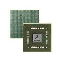
MPC8544VTALF Freescale Semiconductor, MPC8544VTALF Datasheet - Page 25

MPC8544VTALF
Manufacturer Part Number
MPC8544VTALF
Description
MPU POWERQUICC III 783-PBGA
Manufacturer
Freescale Semiconductor
Datasheets
1.MPC8544VTALF.pdf
(117 pages)
2.MPC8544VTALF.pdf
(2 pages)
3.MPC8544VTALF.pdf
(1340 pages)
Specifications of MPC8544VTALF
Processor Type
MPC85xx PowerQUICC III 32-Bit
Speed
667MHz
Voltage
1V
Mounting Type
Surface Mount
Package / Case
783-FCPBGA
Processor Series
MPC85xx
Core
e500
Data Bus Width
32 bit
Maximum Clock Frequency
667 MHz
Maximum Operating Temperature
+ 105 C
Mounting Style
SMD/SMT
Data Ram Size
32 KB
I/o Voltage
1.8 V, 3.3 V
Interface Type
I2C, HSSI, DUART
Minimum Operating Temperature
0 C
Lead Free Status / RoHS Status
Lead free / RoHS Compliant
Features
-
Lead Free Status / Rohs Status
Lead free / RoHS Compliant
Available stocks
Company
Part Number
Manufacturer
Quantity
Price
Company:
Part Number:
MPC8544VTALF
Manufacturer:
Freescale Semiconductor
Quantity:
10 000
Company:
Part Number:
MPC8544VTALFA
Manufacturer:
Freescale Semiconductor
Quantity:
10 000
8.3
Each SGMII port features a 4-wire AC-coupled serial link from the dedicated SerDes 2 interface of
MPC8544E as shown in
pin of the SerDes transmitter differential pair features 50-Ω output impedance. Each input of the SerDes
receiver differential pair features 50-Ω on-die termination to SGND_SRDS2 (xcorevss). The reference
circuit of the SerDes transmitter and receiver is shown in
When an eTSEC port is configured to operate in SGMII mode, the parallel interface’s output signals of
this eTSEC port can be left floating. The input signals should be terminated based on the guidelines
described in
the desired POR configuration requirement on these pins, if applicable.
When operating in SGMII mode, the eTSEC EC_GTX_CLK125 clock is not required for this port. Instead,
SerDes reference clock is required on SD2_REF_CLK and SD2_REF_CLK pins.
8.3.1
Table 23
SD2_REF_CLK are not intended to be used with, and should not be clocked by, a spread spectrum clock
source.
8.3.2
Table 24
characteristics. Transmitter DC characteristics are measured at the transmitter outputs (SD2_TX[n] and
SD2_TX[n]) as depicted in
Freescale Semiconductor
Supply Voltage
Output high voltage
Output low voltage
Output ringing
Note:
1. 8 ns applies only when 125 MHz SerDes2 reference clock frequency is selected via cfg_srds_sgmii_refclk during POR.
Symbol
t
t
REFCJ
REFPJ
t
REF
Parameter
lists the SGMII SerDes reference clock AC requirements. Please note that SD2_REF_CLK and
and
SGMII Interface Electrical Characteristics
REFCLK cycle time
REFCLK cycle-to-cycle jitter. Difference in the period of any
two adjacent REFCLK cycles
Phase jitter. Deviation in edge location with respect to
mean edge location
AC
SGMII Transmitter and Receiver DC Electrical Characteristics
Section 21.5, “Connection Recommendations,”
Table 25
MPC8544E PowerQUICC III Integrated Processor Hardware Specifications, Rev. 5
Requirements for SGMII SD2_REF_CLK and
Table 23. SD2_REF_CLK and SD2_REF_CLK AC Requirements
describe the SGMII SerDes transmitter and receiver AC-coupled DC electrical
Figure
Parameter Description
Figure
Table 24. DC Transmitter Electrical Characteristics
V
Symbol
DD_SRDS2
V
V
V
7, where C
RING
OH
OL
8.
V
OS
TX
-min –|V
is the external (on board) AC-coupled capacitor. Each output
0.95
Min
—
—
OD
|
-max
/2
Figure
Enhanced Three-Speed Ethernet (eTSEC), MII Management
Typ
1.0
—
—
—
as long as such termination does not violate
Min
–50
—
—
7.
V
OS
-max + |V
Typical
10 (8)
—
—
Max
1.05
10
—
SD2_REF_CLK
OD
|
–max
Max
100
50
—
/2
Unit
mV
mV
%
V
Units
ns
ps
ps
Notes
—
—
Notes
1
—
—
1
25


