DP83905AVQB National Semiconductor, DP83905AVQB Datasheet - Page 74
DP83905AVQB
Manufacturer Part Number
DP83905AVQB
Description
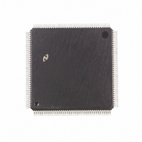
IC CONTROLR AT/LAN TP IN 160PQFP
Manufacturer
National Semiconductor
Series
AT/LANTIC™r
Datasheet
1.DP83905AVQB.pdf
(80 pages)
Specifications of DP83905AVQB
Controller Type
AT, LAN Twisted-Pair Interface Controller
Voltage - Supply
4.75 V ~ 5.25 V
Current - Supply
100mA
Operating Temperature
0°C ~ 70°C
Mounting Type
Surface Mount
Package / Case
160-BFQFP
Lead Free Status / RoHS Status
Contains lead / RoHS non-compliant
Interface
-
Other names
*DP83905AVQB
Available stocks
Company
Part Number
Manufacturer
Quantity
Price

Company:
Part Number:
DP83905AVQB
Manufacturer:
Texas Instruments
Quantity:
10 000
Part Number:
DP83905AVQB
Manufacturer:
NS/国半
Quantity:
20 000


Symbol
T22
T23
T24
T25
T26
T27
T28a
T28b
T29
T30
T31
T32
T33
T34
T35a
T35b
T36a
T36b
T37
T38a
T38b
8 0 Preliminary Switching Characteristics
ISA Slave Accesses
Note 1 M16 IO16 are only asserted for 16-bit transfers
Note 2 CHRDY is only deasserted if the NIC core can not service the access immediately It is held deasserted until the NIC core is ready causing the system to
insert wait states
Note 3 On 8-bit transfers only 8 bits of MSD0–15 and D0–7 are driven
Note 4 This is the early CHRDY timing required by some machines where CHRDY is referenced to BALE In this mode of operation under certain circumstances
CHRDY will be asserted for cycles which are not for this device i e memory cycles or I O cycles where SA0–9 match our address before reaching their valid state
In such a case the time to assert CHRDY from MRD MWR or SA0–9 invalid will be the same as the deassertion time specified
Note 5 This is the standard CHRDY timing where CHRDY is asserted after IORD or IOWR
Note 6 Read data valid is referenced to CHRDY when wait states have been inserted
Note 7 If no wait states are inserted read data valid can be measured from IORD
Note 8 This is a minimum timing with no additional wait states
Note 9 This is the standard IO16 timing where IO16 is asserted after a valid address decode
Note 10 This is the late IO16 timing required by some machines where IO16 is asserted after a valid address decode and IORD or IOWR going active
Note 11 This is a timing for a RAM access
Note 12 RCS refers to RCS1 and RCS2 Depending on the mode of operation either or both can be asserted See the Functional Bus Timing section for a further
explanation
Note 13 This is a timing for a Boot PROM access
BALE Deasserted before LA17–23 Invalid
LA17–23 Valid before MRD MWR Asserted
Read Data Valid on MSD0–15 to Valid on SD0–15
MSRD Deasserted to MSD0–15 Read Data Invalid (Note 3)
Write Data Valid on SD0–15 to Valid on MSD0–15
SA0–19 Valid to RCS or BPCS Asserted (Note 11)
MRD Asserted to MSRD Asserted
MWR Asserted to MSWR Asserted
SA0–19 Valid to MSA1–15 Valid
SA0–19 Invalid to RCS or BPCS Deasserted (Note 11)
MRD SMRD Deasserted to MSRD Deasserted
MSWR Deasserted to MA1
MSWR Deasserted to MSD0–15 Invalid (Note 3)
MSA1–15 valid before MSWR Asserted
RCS Asserted to CHRDY Asserted (Note 11 12)
BPCS Asserted to CHRDY Asserted (Note 13)
MSRD MSWR Asserted to CHRDY Asserted (Note 11)
MSRD MSWR Asserted to CHRDY Asserted (Note 13)
MSA1–15 Valid to CHRDY Asserted (Note 11)
Driving Data from SD0–15 on to MSD0–15
to CHRDY Asserted (Note 11)
Driving Data from SD0–15 on to MSD0–15
to CHRDY Asserted (Note 13)
Description
b
15 Invalid
74
(Continued)
Min
175
150
260
10
20
80
15
75
60
0
0
0
0
Transfers
8-Bit
Max
120
70
65
55
60
60
Min
175
150
260
40
10
20
80
15
75
60
0
0
0
0
0
Transfers
16-Bit
Max
120
70
65
55
60
60
Units
ns
ns
ns
ns
ns
ns
ns
ns
ns
ns
ns
ns
ns
ns
ns
ns
ns
ns
ns
ns
ns
Related parts for DP83905AVQB
Image
Part Number
Description
Manufacturer
Datasheet
Request
R

Part Number:
Description:
AT Local Area Network Twisted-Pair Interface Controller
Manufacturer:
National Semiconductor
Datasheet:

Part Number:
Description:
NIC Network Interface Controller
Manufacturer:
NSC [National Semiconductor]
Datasheet:
Part Number:
Description:
National Semiconductor [8-Bit D/A Converter]
Manufacturer:
National Semiconductor
Datasheet:
Part Number:
Description:
National Semiconductor [Media Coprocessor]
Manufacturer:
National Semiconductor
Datasheet:
Part Number:
Description:
Digitally Controlled Tone and Volume Circuit with Stereo Audio Power Amplifier, Microphone Preamp Stage and National 3D Sound
Manufacturer:
National Semiconductor
Datasheet:
Part Number:
Description:
Digitally Controlled Tone and Volume Circuit with Stereo Audio Power Amplifier, Microphone Preamp Stage and National 3D Sound
Manufacturer:
National Semiconductor
Datasheet:
Part Number:
Description:
AC97 Rev 2 Codec with Sample Rate Conversion and National 3D Sound
Manufacturer:
National Semiconductor
Part Number:
Description:
Manufacturer:
National Semiconductor
Datasheet:
Part Number:
Description:
Manufacturer:
National Semiconductor
Datasheet:
Part Number:
Description:
General Purpose, Low Voltage, Low Power, Rail-to-Rail Output Operational Amplifiers
Manufacturer:
National Semiconductor
Datasheet:
Part Number:
Description:
8-bit 20 MSPS flash A/D converter.
Manufacturer:
National Semiconductor
Datasheet:
Part Number:
Description:
Low Noise Quad Operational Amplifier
Manufacturer:
National Semiconductor
Datasheet:
Part Number:
Description:
Quad Differential Line Receivers
Manufacturer:
National Semiconductor
Datasheet:
Part Number:
Description:
Quad High Speed Trapezoidal? Bus Transceiver
Manufacturer:
National Semiconductor
Datasheet: