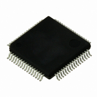
VSC8601XKN Vitesse Semiconductor Corp, VSC8601XKN Datasheet - Page 11

VSC8601XKN
Manufacturer Part Number
VSC8601XKN
Description
IC PHY 10/100/1000 64-EP-LQFP
Manufacturer
Vitesse Semiconductor Corp
Type
PHY Transceiverr
Specifications of VSC8601XKN
Number Of Drivers/receivers
1/1
Protocol
Gigabit Ethernet
Voltage - Supply
2.5V, 3.3V
Mounting Type
Surface Mount
Package / Case
64-LQFP Exposed Pad, 64-eLQFP, 64-HLQFP
Case
TQFP
Dc
06+
Lead Free Status / RoHS Status
Lead free / RoHS Compliant
Other names
907-1028
Available stocks
Company
Part Number
Manufacturer
Quantity
Price
Company:
Part Number:
VSC8601XKN
Manufacturer:
KYOCERA/AVX
Quantity:
20 000
Company:
Part Number:
VSC8601XKN
Manufacturer:
VITESSE
Quantity:
1 235
Company:
Part Number:
VSC8601XKN
Manufacturer:
Vitesse Semiconductor Corporation
Quantity:
10 000
Part Number:
VSC8601XKN
Manufacturer:
VITESSE
Quantity:
20 000
Revision 2.1
Revision 4.1
September 2009
•
•
•
•
•
•
Revision 2.1 of this datasheet was published in February 2006. The following is a
summary of the changes implemented in the datasheet:
•
•
•
•
•
•
•
•
•
•
they were inadvertently added in a prior revision of this document. The I
I
For the 100BASE current consumption specifications, all references to the speed
were corrected from 100BASE-X to 100BASE-TX.
In the AC characteristics for the CLKOUT pin, the total jitter specifications were
added. They are 217 ps typical and 491 ps maximum.
For device reset, both the reset characteristics and timing diagram were updated to
include new parameters: reset rise time (t
(t
In the stress ratings, the power supply voltage parameter was removed because it
was redundant.
In the pin description for TX_CLK, the rate was clarified to be 2.5 MHz for 10 Mbps
mode, 25 MHz for 100 Mbps mode, or 125 MHz for 1000 Mbps mode.
The errata item “RX_CLK Can Reach as High as 55% Duty Cycle” remains in effect
but all other errata items no longer apply to the latest part revision.
In the high-level block diagram, representation of the XTAL pin was corrected from
“XTAL 1/2” to “XTAL1” and “XTAL2.”
In the RGMII to Cat5 block diagram, the interface name was corrected from GMII to
RGMII.
New information was added about how to manually force the device to use
MDI/MDI-X.
The VSC8601 device switches between the low-power state and LP wake-up state
every two seconds; the rate is not programmable, as was originally stated.
In the link partner wake-up state, the device sends FLP bursts for two seconds;
they are not limited to three bursts, as was originally stated.
In the description of the PHY address for the serial management interface (SMI),
the physical address was corrected from 3:0 to 4:0.
For the enhanced LED method, controlled by MII Register 16E, two of the LED
modes have changed. Mode 11, TX activity, and mode 13, RX activity, are now both
reserved.
In the description of the far-end loopback testing feature, the controlling register
bit was corrected from 23.3 to 27E.10.
For the JTAG interface instructions EXTEST and SAMPLE/PRELOAD, the values for
register width were modified from TBD to 45.
For the Mode Control register (address 0), when bit 11 (power-down) is set, RGMII
in-band signaling will not function.
VDD12A
VDDSTABLE
values are kept for current consumption with the regulator disabled.
).
RST_RISE
) and supply stable time
VSC8601 Datasheet
Revision History
VDD12
Page 11
and


