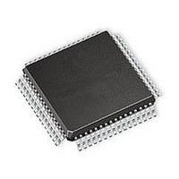
ST92T163R4T1 STMicroelectronics, ST92T163R4T1 Datasheet - Page 146

ST92T163R4T1
Manufacturer Part Number
ST92T163R4T1
Description
Microcontrollers (MCU) OTP EPROM 20K USB/I2
Manufacturer
STMicroelectronics
Datasheet
1.ST92T163R4T1.pdf
(224 pages)
Specifications of ST92T163R4T1
Data Bus Width
8 bit, 16 bit
Program Memory Type
EPROM
Program Memory Size
20 KB
Data Ram Size
2 KB
Interface Type
I2C, SCI, USB
Maximum Clock Frequency
24 MHz
Number Of Programmable I/os
64
Number Of Timers
2
Operating Supply Voltage
4 V to 5.5 V
Maximum Operating Temperature
+ 70 C
Mounting Style
SMD/SMT
Package / Case
TQFP-64
Minimum Operating Temperature
0 C
On-chip Adc
8 bit
Lead Free Status / Rohs Status
No
Available stocks
Company
Part Number
Manufacturer
Quantity
Price
Company:
Part Number:
ST92T163R4T1L
Manufacturer:
ST
Quantity:
444
Part Number:
ST92T163R4T1L
Manufacturer:
ST
Quantity:
20 000
ST92163 - USB PERIPHERAL (USB)
USB INTERFACE (Cont’d)
8.3.4.3 Miscellaneous Registers
These registers contain device configuration pa-
rameters or optional functions of USB interface.
DEVICE CONFIGURATION 1 (DEVCONF1)
R244 - Read/Write
Register page: 60
Reset value: 0000 1111 (0Fh)
This register contains device configuration data
that should be written by the software at the begin-
ning of the application program and should never
be changed during normal operations.
Bit 7:6 = Reserved. This bit is fixed by hardware at
0.
Bit 6 = Reserved. Must be kept at 0.
Bit 5 = USBOE_EN: USBOE Signal Enable .
Set by software to enable the alternate output
function connected to the upstream output enable
signal.
1: USBOE signal output enabled
0: USBOE signal output disabled
Bit 4 = Reserved.
146/224
7
0
-
USBOE
_EN
DEVICE
LS_
1
1
1
0
1
Bits 3:0 = Reserved. These bits are fixed by hard-
ware at 1.
DEVICE CONFIGURATION 2 (DEVCONF2)
R245 - Read/Write
Register page: 60
Reset value: 0000 0000 (00h)
This register contains device configuration data
that should be written by the software at the begin-
ning of the application program and should never
be changed during normal operations.
Bits 7:2 = Reserved. These bits must be always
written to 0.
Bit 1 = LVD_DISABLE: Low Voltage Detector Dis-
able
Set by the software to disable the generation of
the device reset signal by the LVD.
1: LVD disabled
0: LVD enabled
If this bit is at 0, an internal reset can be issued
both by the external RESET pin and the LVD when
it detects a low supply voltage; if this bit is at 1 only
the external pad can start a device reset.
Note: this bit can be only set to 1 by software, writ-
ing 0 has no effect and the LVD can be re-enabled
only using a device reset.
7
0
0
0
0
0
0
DISAB LE
LVD_
ENABLE
SOFP_
0


